VS 2001
Technical Handbook
Accessories
P/N: 779-0373/02
Revision 02
Marconi Proprietary information
Page 41
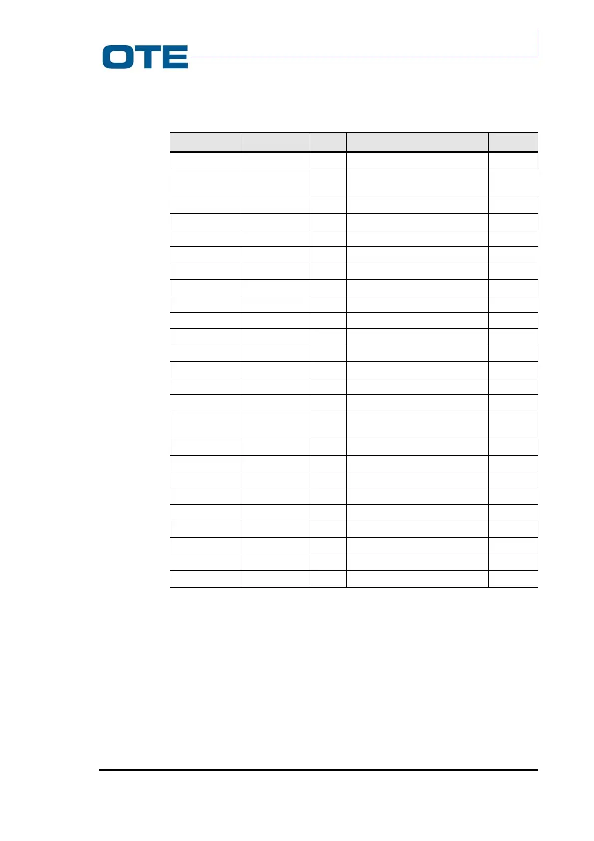
Tab. 2.5: Pins function of J02 connector
Signal Pin Type Description Level
+8V 1,36 POW stabilised voltage for R/T card 7.2 V
GND
2,3,17,18,20,
31,32,33,34,35
POW
ground
Ground
CK2304DA 4 IN serial clock BB. Tx data 0- 3.3 V
LATCH 5 IN timing signal BB Tx data 0 - 3.3 V
ITXD 6 IN serial data component “I” BB Tx 0 - 3.3 V
QTXD 7 IN serial data component “Q” BB Tx 0 - 3.3 V
HIQRXAD 29 OUT serial data i/q BB. Tx 0 – 5 V
HFLGIQ 28 OUT timing serial data BB Tx 0 – 5 V
HCK4608 27 IN master clock for AD7013 0 – 5 V
HCK2304AD 26 OUT control clock data AD7013 0 – 5 V
HDATAAD 25 IN serial control data AD7013 0 – 5 V
HFRAMEAD 24 IN timing control data AD7013 0 – 5 V
SD 8 IN on/off circuits R/T card; 1=off 0 - 3.3 V
TXON 9 IN Tx on/off circuits R/T card Open Coll
RXON
30
IN
Rx on/off circuits R/T card
Open Coll
HDATASER 13 IN serial data for EEPROM, synth,
DAC
0 – 5 V
HCKSER 12 IN serial clock for hdataser 0 – 5 V
HENSINT 16 IN enable for synthesiser 0 – 5 V
HENDAC 14 IN enable for DAC 0 – 5 V
HENEEPROM 15 IN enable for EEPROM 0 – 5 V
SERDATAIN 11 OUT EEPROM data output serial 0 – 5 V
Fref 19 OUT 12.8 MHz reference clock 1 Vpp
BSW 21 IN band switch for VCO WB Open Coll
PAON 10 IN on/off preamp of P.A.; 1=off Open Coll
LD 22 OUT PLL hook up monitor; 0=ok 0 – 5 V
2.3.3 P.A. card
The TETRA vehicular amplifier is housed on the solder side of the R/T card near
the dissipation fins. The P.A. card amplifies the RF input signal coming from the
R/T card in order to supply a power output of 40 dBm in the vehicular radio
operating frequency range (the operating frequency range is different according to
the VS 2001 different versions: see Tab. 1.2). The RF signal amplification is
obtained via a line that consists of a bipolar technology transistor polarised in class
AB, driven by an LDMOS technology power module.