VS 2001
Technical Handbook
Technical Description
Page 40 Marconi Proprietary information
P/N: 779-0373/02
Revision 02
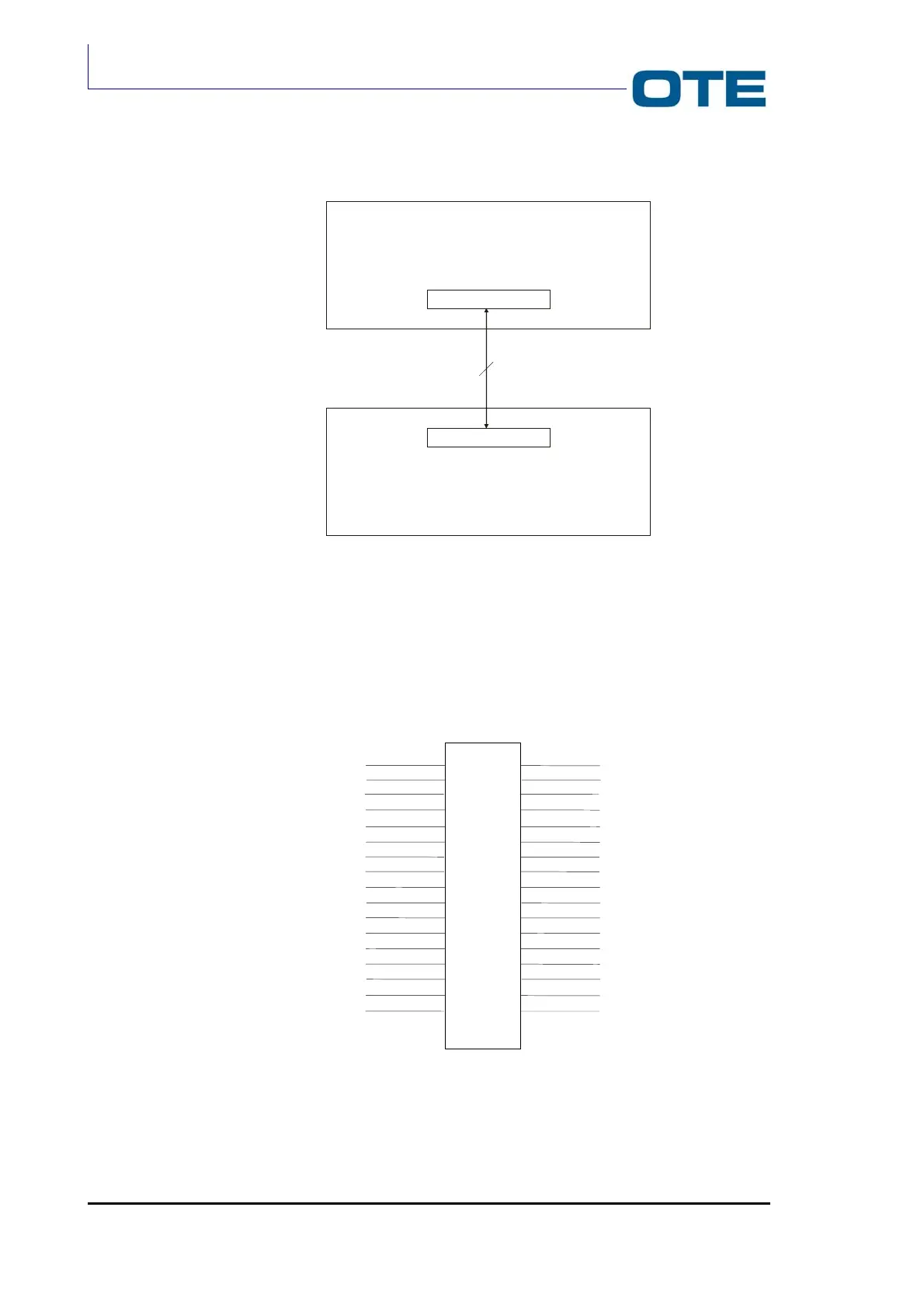
Fig. 2.11: Connection between R/T card and Base Band card
In Fig. 2.12 the J02 connector pin allocation is shown. Note that the J15 connector
on the R/T card is the mirror image of the J02 connector on the Base Band card.
Fig. 2.12: J02 description
In Tab. 2.5 the J02 connector pins function is reported.
1
2
3
4
5
6
7
8
9
10
11
12
13
14
15
16
17
18
36
35
34
33
32
31
30
29
28
27
26
25
24
23
22
21
20
19
+8V
GND
GND
CK2304DA
LATCH
ITXD
QTXD
SD
TXON
PAON
SERDATAIN
HCKSER
HDATASER
HENDAC
HENEEPROM
HENSINT
GND
GND
+8
GND
GND
GND
GND
GND
RXON
HIQRXAD
HFLGI
HCK4608
HCK2304A
HDATAAD
HFRAMEAD
GND
LD
BSW
GND
FREF
R/T CARD
J15 CONNECTOR
36
J02 CONNECTOR
BASEBAND CARD