VS 2001
Technical Handbook
Accessories
P/N: 779-0373/02
Revision 02
Marconi Proprietary information
Page 43
The signal is then adapted and connected to U7 and U6 (transistors LDMOS).
Together with Q1 U7 and U6 are AB class amplifiers whose polarization is fixed by
using the trimmers R51, R37 and R21 respectively.
After the received signal has been properly amplified, it is routed to the RX/TX
switch that is connected, during the receiving phase, to the antenna (J15
connector).
The RF signal is then splitted, by using a directional coupler, into the R/T module
for RF treatment (J16 connector) and to an additional port for ROS monitoring
(VSWR Detector).
Finally, downstream the directional coupler, the signal enters a low-pass filter
(LPF) and then it is connected directly to the antenna (J17 connector).
2.3.3.2
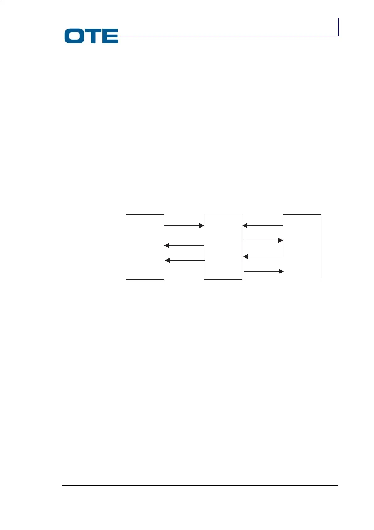
P.A. card Interfacing
The P.A. card interfaces with the R/T card and with the Base Band card as shown
in Fig. 2.14.
Fig. 2.14: P.A. card interfacing
The signals exchanged between the P.A. card and the R/T card are:
RF FEEDBACK signal
This signal is picked up directly from the RF signal through the directional coupler
and it is transmitted to the R/T card through the J16 connector. The signal power is
equal to 10dBm.
RFIN signal
This signal is the input (through the J14 connector) of the P.A. line up loop. The
signal power is less than +10dBm.
RF RECEIVED signal
This signal is the RF signal received at the antenna and sent to the receiver
through the J15 connector.
The signals exchanged between P.A. card and Base Band card are:
R/T P.A. BB
RFIN
RFFEEDBACK
RFRECEIVED
PAO N
VSWR
12.5V
RFOUT
BOARD BOARD BOARD