VS 2001
Technical Handbook
Technical Description
Page 42 Marconi Proprietary information
P/N: 779-0373/02
Revision 02
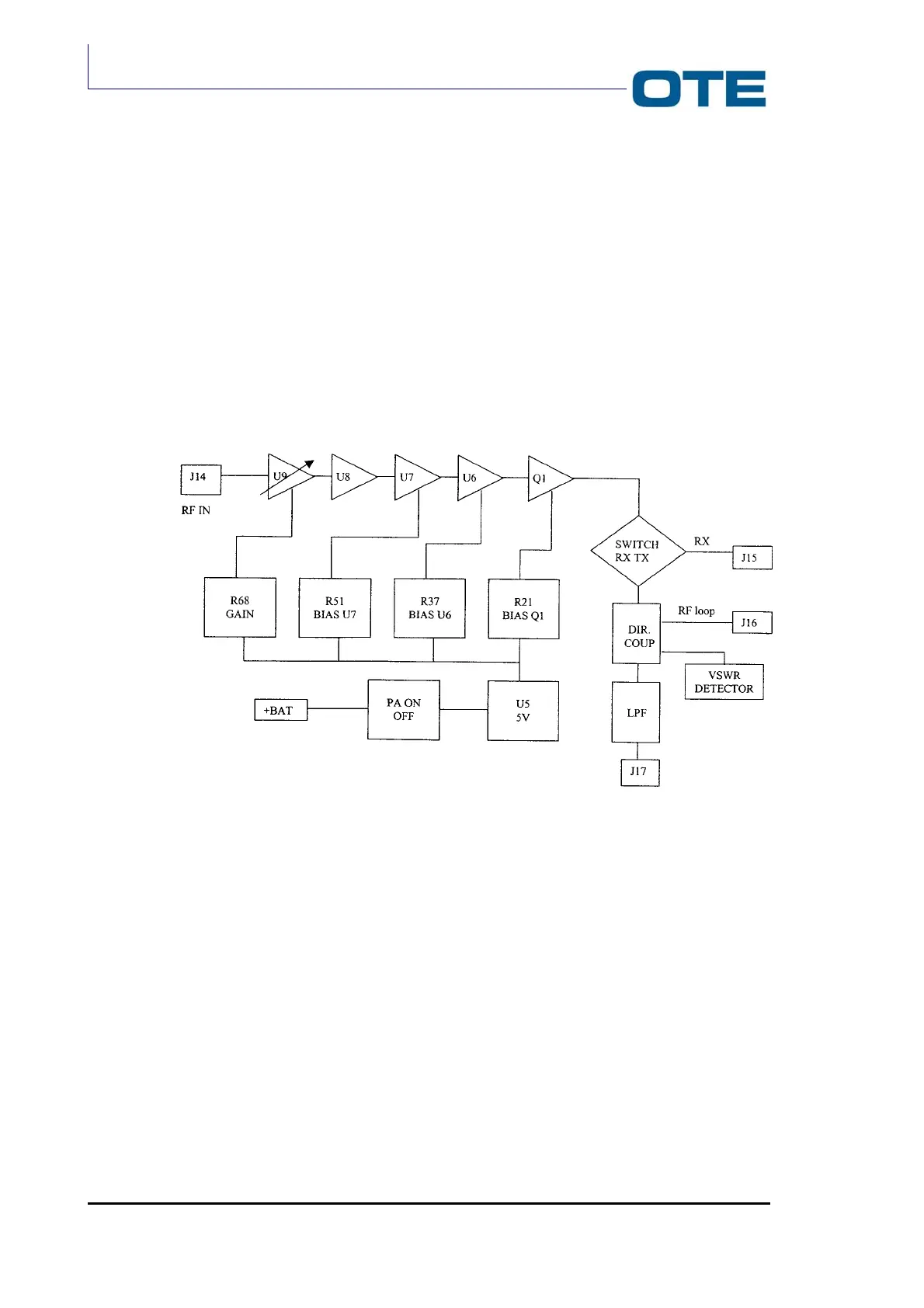
The P.A. card interfaces with the Base Band card through the J06 connector. It
also interfaces with the R/T CARD through the MCX type radio-frequency
connectors: J14, J15 and J16. The J14 connector provides the RF signal input
from the VCO. The J15 connector carries the signal from the antenna to the
receiver input. The J16 connector returns the RF signal output to the R/T card and
provides the linearization of the modulation. The amplified radio-frequency signal
exits on the J17 connector and, through proper cable, is connected to the antenna.
2.3.3.1
Functional description
The block diagram of the P.A. card is shown in Fig. 2.13.
Fig. 2.13: Block diagram of the P.A. card
The PA ON OFF is switched on and off by acting directly on the 12 V line where a
P channel MOSFET with low RDS(on) is inserted.
When the signal PAON (see par. 2.3.3.2) is at high logic level: VTX = 12 V and
VRX = 0. When PA ON is at low logic level the values are inverted.
The main task of the PA ON OFF module is to amplify the RF signal generated by
the RT module up to 10 W in the vehicular radio operating frequency range (see
Tab. 1.2).
The RF signal generated by the R/T module, via the J14 connector, is applied to
the first step U9 (variable gain amplifier) used to set PA card gain by means of the
R68 network (see Fig. 2.13).
Then the signal is applied to the second step U8 (monolithic amplifier) where it is
further amplified in order to drive properly the subsequent steps.