RL78/F13, F14 CHAPTER 26 VOLTAGE DETECTOR
R01UH0368EJ0210 Rev.2.10 1564
Dec 10, 2015
26.3.2 Voltage detection level register (LVIS)
This register selects the voltage detection level.
This register can be set by a 1-bit or 8-bit memory manipulation instruction.
Reset signal generation input sets this register to 00H/01H/81H
Note1
.
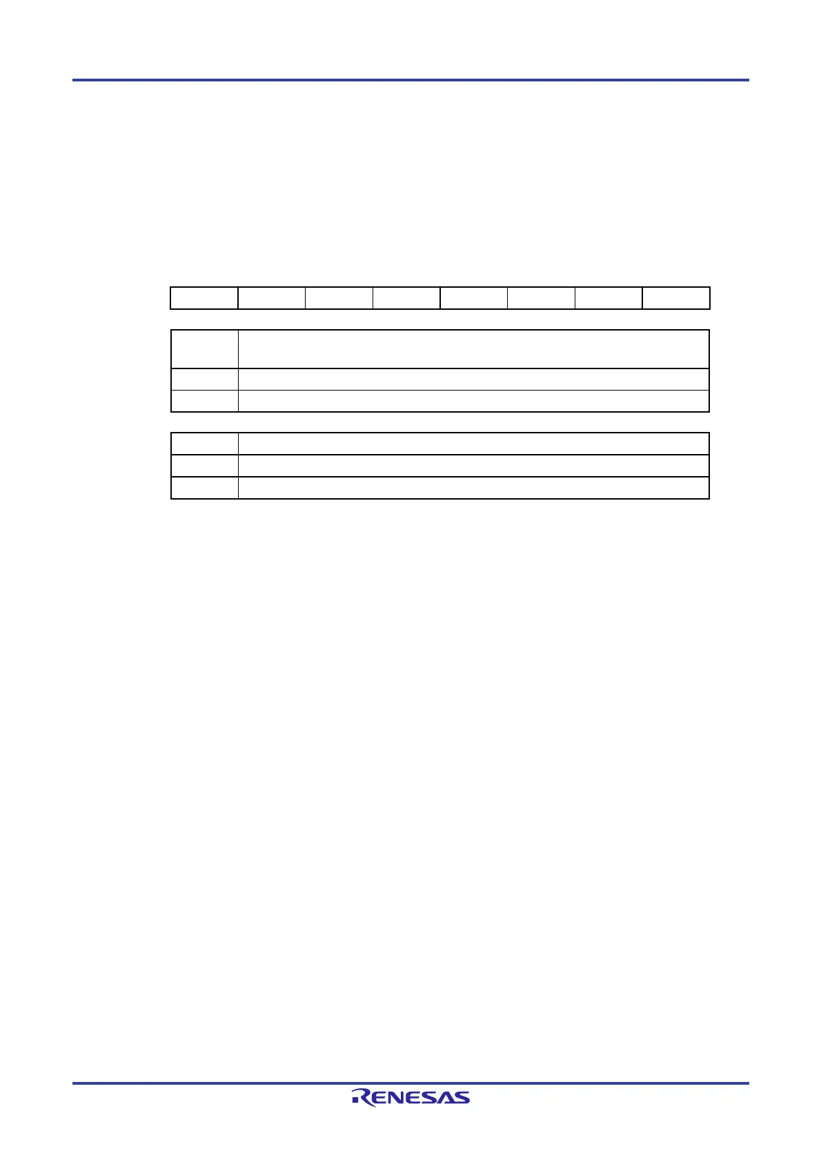
Figure 26-3. Format of Voltage Detection Level Register (LVIS)
Address: FFFAAH After reset: 00H/01H/81H
Note 1
R/W
Symbol <7> 6 5 4 3 2 1 <0>
LVIS LVIMD 0 0 0 0 0 0 LVILV
LVIMD
Note
2
Operation mode of voltage detection
0 Interrupt mode
1 Reset mode
LVILV
Note 2
LVD detection level
0 High-voltage detection level (VLVDH)
1 Low-voltage detection level (VLVDL or VLVD)
Notes 1. The reset value changes depending on the reset source and the setting of the option byte.
This register is not cleared (00H) by LVD reset.
The generation of reset signal other than an LVD reset sets as follows.
When option byte LVIMDS1, LVIMDS0 = 1, 0: 00H
When option byte LVIMDS1, LVIMDS0 = 1, 1: 81H
When option byte LVIMDS1, LVIMDS0 = 0, 1: 01H
2. Writing 0 can only be allowed when LVIMDS1 and LVIMDS0 are set to 1 and 0 (interrupt and reset mode)
by the option byte. In other cases, writing is not allowed and the value is switched automatically when reset
or interrupt is generated.
Cautions 1. Only rewrite the value of the LVIS register after setting the LVISEN bit (bit 7 of the LVIM register) to 1.
2. Specify the LVD operation mode and detection voltage (V
LVDH, VLVDL) by using the option byte (000C1H).
Table 26-1 shows the option byte (000C1H) settings. For details about the option byte, see CHAPTER
29 OPTION BYTE.
 Loading...


