RL78/F13, F14 CHAPTER 8 TIMER RD
R01UH0368EJ0210 Rev.2.10 576
Dec 10, 2015
8.2.7 Timer RD Function Control Register (TRDFCR)
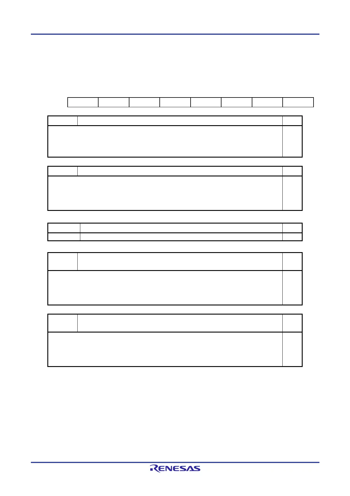
Figure 8-8. Format of Timer RD Function Control Register (TRDFCR)
Address: F0266H After Reset: 80H
Note 1
Symbol 7 6 5 4 3 2 1 0
TRDFCR PWM3
STCLK 0 0 OLS1
OLS0 CMD1 CMD0
PWM3
PWM3 mode select
Note 2
R/W
In the timer mode, set to 1 (other than PWM3 mode).
In PWM3 mode, set to 0 (PWM3 mode).
Disabled in reset synchronous and complementary PWM modes.
R/W
STCLK External clock input select R/W
In the timer mode, the reset synchronous PWM mode, and the complementary PWM mode,
0: External clock input disabled
1: External clock input enabled
In PWM3 mode, set to 0 (external clock input disabled).
R/W
OLS1 Counter-phase output level select
(in reset synchronous PWM mode or complementary PWM mode)
R/W
In reset synchronous and complementary PWM modes,
0: High initial output and low active level
1: Low initial output and high active level
Disabled in timer and PWM3 modes.
R/W
OLS0 Phase output level select
(in reset synchronous PWM mode or complementary PWM mode)
R/W
In reset synchronous and complementary PWM modes,
0: High initial output and low active level
1: Low initial output and high active level
Disabled in timer and PWM3 modes.
R/W
Bits 5 to 4
Reserved R/W
0 Set to 0. R/W
 Loading...


