RL78/F13, F14 CHAPTER 3 CPU ARCHITECTURE
R01UH0368EJ0210 Rev.2.10 198
Dec 10, 2015
Figure 3-65. Example of POP
Figure 3-66. Example of CALL, CALLT
SP
(SP+1)
(SP)
F0000H
POP rp
SP
+1
SP
SP
SP
+2
rp
OP-code
<1>
<1>
<2>
<2>
Stack
area
Memory
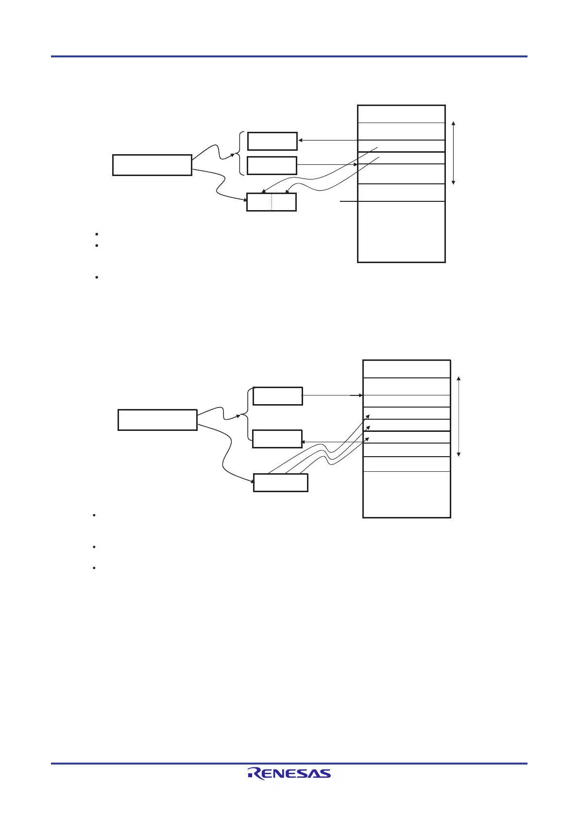
Stack addressing is specified <1>.
The contents of addresses SP and SP + 1 are stored in the
lower-order and higher-order bytes of the pair of registers
indicated by rp <2>, respectively.
The value of SP <3> is increased by two (if rp is the program
status word (PSW), the content of address SP + 1 is stored in
the PSW).
Instruction code
CALL
00H
SP
F0000H
PC
SP
SP
-
1
SP
-
2
SP
-
3
SP
-
4
OP-code
<1>
<1>
<2>
Stack
area
Memory
Instruction code
<3>
Stack addressing is specified <1>. The value of the program
counter (PC) changes to indicate the address of the instruction
following the CALL instruction.
00H, the values of PC bits 19 to 16, 15 to 8, and 7 to 0 are stored
in addresses SP - 1, SP - 2, SP - 3, and SP - 4, respectively <2>.
The value of the SP <3> is decreased by 4.
PC19 - PC16
PC15 - PC8
PC7 -
PC0
 Loading...


