RL78/F13, F14 CHAPTER 5 CLOCK GENERATOR
R01UH0368EJ0210 Rev.2.10 401
Dec 10, 2015
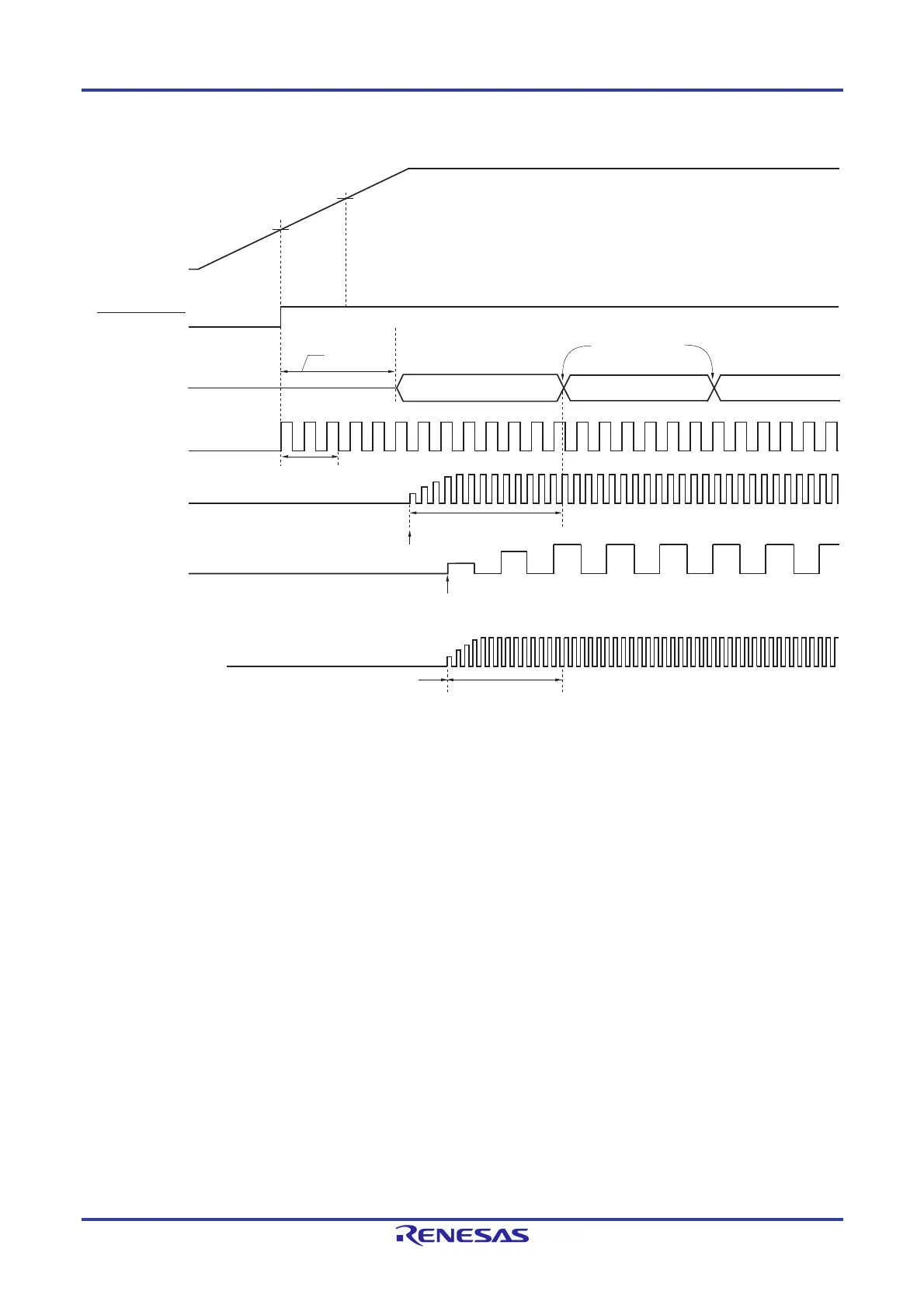
Figure 5-26. Clock Generator Operation When Power Supply Voltage Is Turned On
<1> When the power is turned on, an internal reset signal is generated by the power-on-reset (POR) circuit.
<2> When the power supply voltage exceeds 1.56 V (TYP.), the reset is released and the high-speed on-chip oscillator
automatically starts oscillation.
<3> The CPU starts operation on the high-speed on-chip oscillator clock after a reset processing such as waiting for
the voltage of the power supply or regulator to stabilize has been performed after reset release.
<4> Set the start of oscillation of the X1 clock, XT1 clock, low-speed on-chip oscillator, or PLL clock via software (see
5.6.2 Example of Setting X1 Oscillator, 5.6.3 Example of Setting XT1 Oscillator, 5.6.4 Examples of Setting
PLL Circuit, or 5.6.5 Example of Setting Low-Speed On-Chip Oscillator).
<5> When switching the CPU clock to the X1 or XT1 clock, wait for the clock oscillation to stabilize, and then set
switching via software (see 5.6.2 Example of Setting X1 Oscillator and 5.6.3 Example of Setting XT1 Oscillator).
Notes 1. The internal reset processing time includes the oscillation accuracy stabilization time of the high-speed on-
chip oscillator clock.
2. When releasing a reset, confirm the oscillation stabilization time for the X1 clock using the oscillation
stabilization time counter status register (OSTC).
3. For details about the reset processing time, see CHAPTER 25 POWER-ON-RESET (POR) CIRCUIT.
4. When the PLL circuit starts operation, time is required so that the PLL circuit becomes locked (LOCK = 1).
Caution It is not necessary to wait for the oscillation stabilization time when an external clock input from the
EXCLK pin is used.
X1 clock
oscillation stabilization time
Note 2
CPU clock
High-speed on-chip oscillator clock High-speed system clock
Switched by software
Subsystem clock
PLL clock (f
PLL
)
Starting X1 oscillation
is specified by software.
Reset processing
Note 3
Internal reset signal
0 V
1.56 V
(TYP.)
2.7 V
<1>
<2>
<3>
<4>
<5>
<5>
<4>
Note 1
<4>
Power supply
voltage (V
DD
)
Starting XT1 oscillation
is specified by software.
Starting PLL oscillation
is specified by software.
PLL clock
oscillation stabilization time
Note 4
High-speed
system clock (f
MX
)
(when X1 oscillation
selected)
Subsystem clock (f
SUB
)
(when XT1 oscillation
selected)
High-speed on-chip
oscillator clock (f
IH
)
 Loading...


