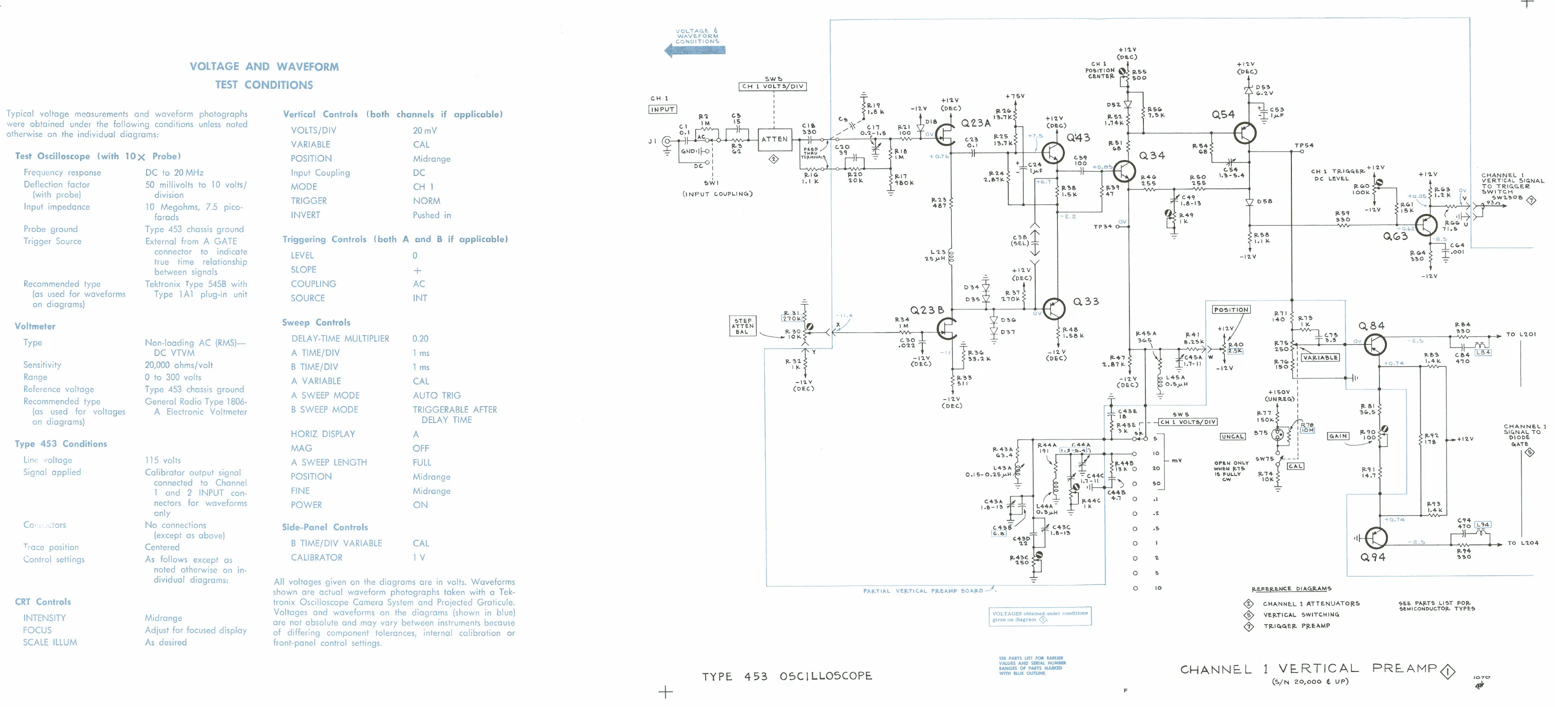
VOLTAGE
AND
WAVEFORM
TEST
CONDITIONS
Typical
voltage measurements
and
waveform photographs
were obtained under the following
conditions
unless
noted
otherwise on the
individual
diagrams:
Test Oscilloscope (with
10
X
Probe)
Frequency response
Deflection factor
(with
probe)
Input
impedance
Probe
ground
Trigger Source
Recommended type
(as
used for waveforms
on diagrams}
Voltmeter
Type
Sensitivity
Range
Reference
voltage
Recommended type
(as
used
for
voltages
on
diagrams}
Type
453
Conditions
Line
:oltage
Signal applied
Co,,
~dors
Trace
position
Control
settings
CRT
Controls
INTENSITY
FOCUS
SCALE
ILLUM
DC
to
20
MHz
50
millivolts
to
l
0 volts/
division
l
0
Megohms, 7.5 pico-
farads
Type
453
chassis ground
External
from
A
GATE
connector to indicate
true time
relationship
between signals
Tektronix
Type
545B
with
Type
lAl
plug-in
unit
Non-loading
AC
(RMS}-
DC
VTVM
20,000 ohms/volt
0
to
300 volts
Type
453
chassis ground
General Radio Type
1806-
A
Electronic Voltmeter
115
volts
Calibrator output signal
connected to Channel
1 and 2
INPUT
con-
nectors for waveforms
only
No connections
(except as above}
Centered
As
follows
except
as
noted otherwise on
in-
dividual diagrams:
Midrange
Adjust for focused display
As
desired
Vertical Controls
(both
VOLTS/DIV
VARIABLE
POSITION
Input
Coupling
MODE
TRIGGER
INVERT
Triggering
Controls
(both
LEVEL
SLOPE
COUPLING
SOURCE
Sweep
Controls
DELAY-TIME
MULTIPLIER
A
TIME/DIV
B
TIME/DIV
A
VARIABLE
A
SWEEP
MODE
B
SWEEP
MODE
HORIZ
DISPLAY
MAG
A
SWEEP
LENGTH
POSITION
FINE
POWER
Side-Panel
Controls
channels
if
20mV
CAL
Midrange
DC
CH
1
NORM
Pushed
in
A
and
0
+
AC
INT
0.
20
1
ms
1
ms
CAL
8
if
applicable)
applicable!
AUTO
TRIG
TRIGGERABLE
AFTER
DELAY
TIME
A
OFF
FULL
Midrange
Midrange
ON
B
TIME/DIV
VARIABLE
CAL
CALIBRATOR
1
V
All
voltages
given
on
the diagrams are
in
volts.
W'aveforms
shown
are
actual
waveform photographs taken with a
Tek-
tronix
Oscilloscope Camera System and Projected
Graticule.
Voltages
and waveforms on the diagrams (shown
in
blue}
are
not
absolute
and may vary between instruments because
of differing component
tolerances, internal
calibration or
front-panel control
settings.
CH
1
VOLTA<;.Fo.
~
WAVE.FORM
~
CONDITION<;.
i
1NPUT
I
I
CH
l
VO~H/DIV
I
-
T~~\
C.!t
..••
J
C l
,....\\
CIT
+1'1V
- 1'2.V
( Df>C.)
p.'2.<0
Q
Z.3A
13.,t<
+ 1
"2V
(DEC.
)
.
~
o.
1
.i-c.
TT
E N
L-...---l
ll...-,,..,...4
"-0-...-
--o-.-!"2''1-
-
1
'-
5
-.-
-'\/\tv-
-+----li::-t--,
C
'l
3
p.
'2.
s
J
I
te...._,.,...._
A./V\
.-+--1
A \
13,
1
I<
-::-
C:.i..JD
•I
f--0
::
~i
.__
0
-l•I-'
----++-_!_-f-l
~
-=-
+0.7"
DC.
I
Q~3
C.3'1
1
00
I
o:.w1
jl-
1
(#
1. 1
I<
JL
l1
~!IOI<
+E:..i
( I
NPUT
C.
DU
PL
I
NC.)
..:.
c.~11
1
(
'!>
E.
L) J
-2.
. 2.
TP'!>"\
Q33
+
-1'2.
v
(
DEC)
-11.<4
y
P.33
5 1 1
- 1'2.V
( DE
C.
)
L-43A
O,
I
S-0.'2.S)-'
H
-1'2.
v
(DE.C
)
-=-
L_
_____________________
-r
-------
____
_
__,
TYPE
453
OSC!LL05COPE.
VOLTAGES
obtalne
d
under
conditions
given
on
diagram
Q>.
SH
PARTS
UST
FOi
EAnH
YAlUl!S
AND
SlltlAl
NU
.....
RANGES
Of
PARTS
MARKED
WITH
llUE
OU1UNE.
+ 1
'2.V
(oe.c.)
av
+ 1
'2.
V
(De.c.)
D
S!I
- 1
'2.
v
POS
IT ION
12.
11
14 0
TPS4
-1
'2.
V
-O.b2
Q<;,3
- 1'2.V
~,
5.,._
_
_.........:.
.:..::_
.....
-=
'-4--
-2
.":>
-
1'2.
v
( DEC. )
T
i3E.
'OW
s
p.
43
E.
r -
...j
c.H
1
VO
LT
S/ DI V !
'2.SO
P.
1
,.
I
SO
l..!-:
--
- - -H
I•
+ l
!'>O
V
:
"'I'-
}
l u
NC."L
I
I:
mV
OPE.W
ONL
Y
'2.0 w H
r.
M
Jl.
1
!>
IS
f.ULL
Y
c.w
!>O
31<
I
~
~
w
~
<;.
W1Sf
1
-;._
-;,_
,
!l-14
IOI<
0
. 1
0
.
~
0
.
!'>
0
0
0
5
0
10
it,E.FE.P..E.NCE 0 1
.i-
Gi
P..
.i-
MS
~
C.
HA
NN
E.L
1
A
TT
E.
N U
AT
OR!>
~
VE.p.TI C..i-L ? WI
TC
HI M
Gi
<!>
TP.
l
<OGiE~
PftEl\MP
CH
A N
NE:.
L
1
V
E..
RT
IC
AL
(5
/ N
20
,
000
t
UP
)
F
Q'i4
-2.":>
fL'l
'l
1
16
+ 1
'2.
V
'l>E.E.
P"
Jl.
T S
LI
':>T
FO
IL
'!>
t M
IC
O>H>
UC.
TOjl,
TV
Pt
'!>
P R
E..A
MP
0
J
0-,.
0
"'*
TO
L
"2
0 1
C HA
NN
E.L
l
S
l
~NAL
T O
DIO
DE.
r..
.i-
r r:
~
TO
L'!.
04