19-1
IM 701310-01E
Specifications
3
2
1
4
5
6
7
8
9
10
11
12
13
14
15
16
17
18
19
App
Index
19.1 Models
Item Specifications
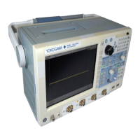
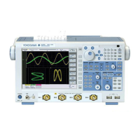
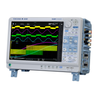
Model name Max. sample rate Frequency bandwidth Max. record length
DL9040 (701307) 5 GS/s 500 MHz 2.5 MW
DL9040L (701308) 5 GS/s 500 MHz 6.25 MW
DL9140 (701310) 5 GS/s 1 GHz 2.5 MW
DL9140L (701311) 5 GS/s 1 GHz 6.25 MW
DL9240 (701312) 10 GS/s 1.5 GHz 2.5 MW
DL9240L (701313) 10 GS/s 1.5 GHz 6.25 MW
19.2 Input Section
Item Specifications
Input channels 4 (CH1 to CH4)
Input coupling setting AC,DC,GND,DC50Ω
Input connector BNC connector
Input impedance 1MΩ±1.0%approx.20pF(10MΩ±2.0%approx.14pFwhenusingPB500passiveprobe)
50Ω±1.5%
Voltage axis sensitivity For1MΩinput: 2 mV/div to 5 V/div (1-2-5 steps)
setting range For50Ωinput: 2 mV/div to 500 mV/div (1-2-5 steps)
Maximum input voltage
For 1 M
W
input (at a frequency of 1 kHz or less):
150 Vrms CAT I
For 50
W
input:
5 Vrms and 10 Vpeak (Not to exceed
either of these values.)
DC offset max. setting range
(With probe attenuation
factor set to 1:1)
For1MΩinput
2 mV/div to 50 mV/div: �1 V
100 mV/div to 500 mV/div: �10 V
1 V/div to 5 V/div: �100 V
For50Ωinput
2 mV/div to 50 mV/div: �1 V
100 mV/div to 500 mV/div: �5 V
Vertical axis (voltage axis) accuracy
DC accuracy
1
For1MΩinput: �(1.5% of 8 div + offset voltage accuracy)
For50Ωinput: �(1.5% of 8 div + offset voltage accuracy)
Offset voltage axis 2 mV/div to 50 mV/div: �(1% of setting value +0.2 mV)
accuracy
1
100 mV/div to 500 mV/div: �(1% of setting value +2 mV)
1 V/div to 5 V/div: �(1% of setting value +20 mV)
Voltage standing wave ratio
(VSWR)
1.5 or less within frequency bandwidth (typical value
4
)
Frequency characteristics
1,2
(–3 dB attenuation point when
sine wave with amplitude
�2 div equivalent is input)
For50Ωinput DL9040/DL9040L DL9140/DL9140L DL9240/DL9240L
0.5 V/div to 10 mV/div: DC to 500 MHz DC to 1 GHz DC to 1.5 GHz
5 mV/div: DC to 400 MHz DC to 750 MHz DC to 1 GHz
2 mV/div: DC to 400 MHz DC to 600MHz DC to 750MHz
For1MΩinput(usingPB500,measuredfromprobetip)
5 V/div to 10 mV/div: DC to 500 MHz DC to 500 MHz DC to 500 MHz
5 mV/div to 2 mV/div: DC to 400 MHz DC to 400 MHz DC to 400 MHz
-3 dB low band attenuation
point for AC coupling
10 Hz or below (1Hz or below using the supplied 10:1 probe)
Skew between channels
(with same setting conditions)
1 ns or below
Residual noise level
3
Larger of 0.4 mVrms or 0.05 div rms (typical value
4
)
Isolation between channels
(at same voltage axis sensitivity)
500 MHz model: –34 dB at 500 MHz (typical value
4
)
1 GHz model: –30 dB at 1 GHz (typical value
4
)
1.5 GHz model: –30 dB at 1.5 GHz (typical value
4
)
A/D conversion resolution 8 bits (25 LSB/div)
Max. 12 bits (in high resolution mode)
Chapter 19 Specifications

 Loading...
