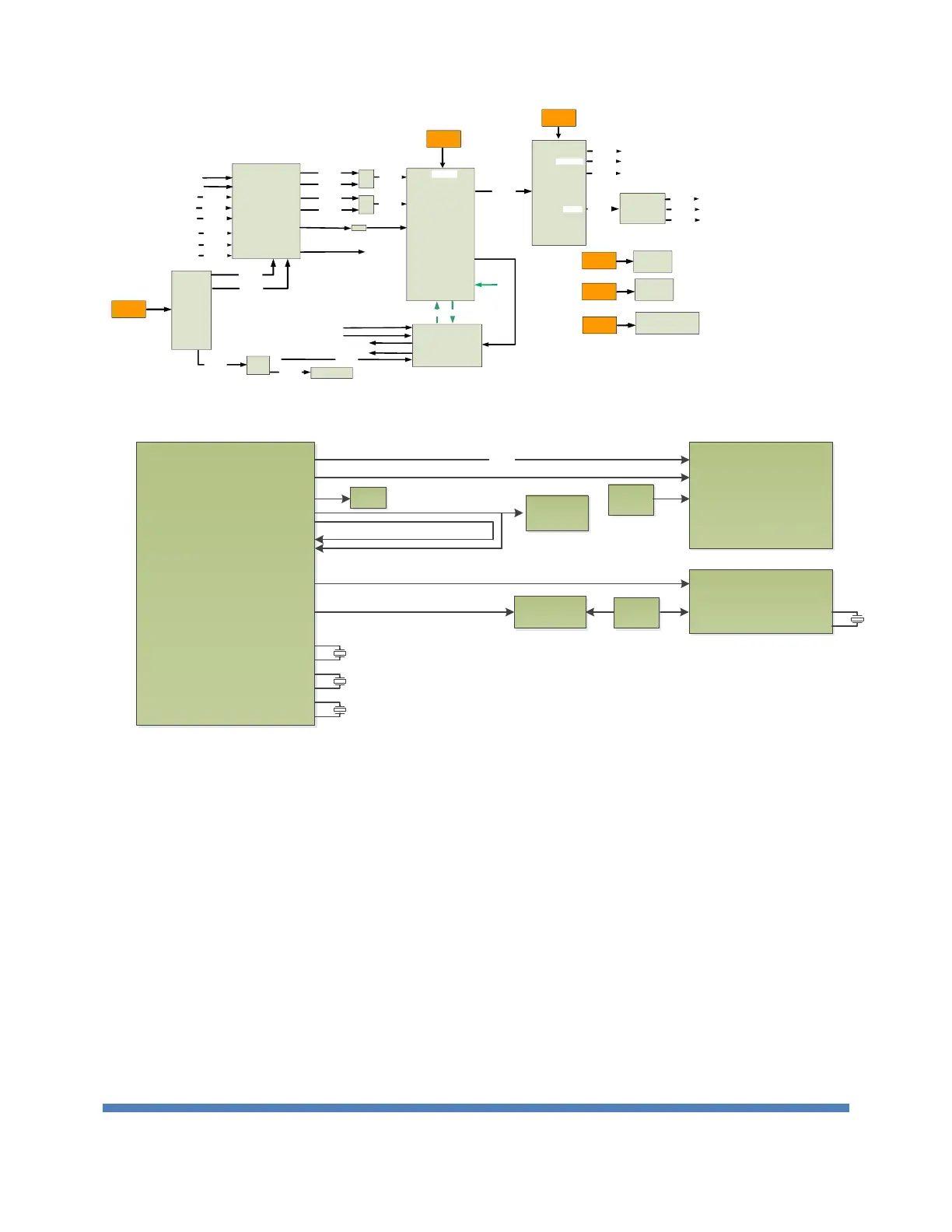
IDT89307
M6163LF
OCXO
Single-End
Single-End
OUT2_P/N
(156MHz)
OUT3_P/N
(25MHz)
IN1_P/N
IN2_P/N
1pps
OUT1
IN3
OSCI
8T49N240
25MHz
XTAL
Differential
Differential
8SLVP1204
1 to 4
Fanout buffer
50MHz
Differential
Differential
50MHz
50MHz
156.25MHz
To 56873 (FC7_8_REFCLK)
Differential
156.25MHz
156.25MHz
To 56873 (FC23_24_REFCLK)
To 56873 (BS_PLL0_REFCLK_RESERVED)
To 56873 (BS_PLL1_REFCLK_RESERVED)
50MHz
156.25MHz
25MHz
XTAL
IDT
5P49V5901
Clock GEN
Differential
50MHz
To 56873 (TS_PLL_REFCLK_RESERVED)
CORE_PLL_REFCLKp/n
Differential
50MHz
PCIE_REFCLKp/n
Differential
100MHz
BCM56873
L1_RCVRD_CLK_BKUP
25MHz
L1_RCVRD_CLK
25MHz
AND
GATE
L1_RCVRD_CLK_VALID
Single-End
Single-End
Single-End
L1_RCVRD_CLK_BKUP_VALID
Single-End
AND
GATE
1pps from CPLD
1PPS_GPIO2
IP_UART 0_SOUT
HCSL
1.4V
CML
1.8V
Differential
Differential
50MHz
50MHz
Differential
156.25MHz
Differential
156.25MHz
Differential
50MHz
FC7_8_REFCL K_p/n
FC23_24_REFCLK_p/n
BS_PL L0_REFCLK_RESE RVED_p/n
BS_PL L1_REFCLK_RESE RVED_p/n
TS_PLL_REFCLK _RESERVED_p/n
1.4V
C
M
L
1.4V
1.8V
1.8V
1.8V
From CPU
IP_UART0_SIN
I2C_0
Rst
Int
L1_RCVRD_CLK_VALID
L1_RCVRD_CLK_VALID_BKUP
25MHz
Jitter:0.17~0.35ps
RMS Jitter Max Requirement:
Core_50M: 10ps
Reference_156.25M: 0.3ps
TS/BS_50M: 10ps
PCIE_100M: 3ps
Jitter: MAX:40fs
Jitter: MAX:40fs
Jitter: MAX:0.7ps
0x54
To MAC
To CPU
IP_TS_GPIO1_3
Res
CPLD3
25MHz
XTAL
USB
HUB
LVPECL
HCSL
100MHz
HCSL
50MHz
LVCMOS
LVCMOS
Single-End
IDT
553MILFT
CPLD2
OUT0_SEL_25M
Single-End
CPLD1_25MHz
Single-End
CPLD2_25MHz
CPLD1
1pps
1PPS
_CLK
1PPS_GPIO2
1PPS_CPU
24MHz
XTAL
50M_CLK_n/QB
25M_DIFF_CLKp/n
IDT8V89307_IN1p/n
IDT8V89307_IN2p/n
OCXO12.8MHz
Clock
PHY
BCM54616S
25MHz
XTAL
Differential
Differential
MC_REFCLK_p/n
Differential
156.25MHz
To 56873 (MC_REFCLK)
1.4V
156.25MHz
To CPU
2.2.2. Power Tree
Based on the power estimation in Table 2, we have to select suitable DC/DC with the
best efficiency as possible.
In addition to convert the voltage from SPS, the regulation of each voltage is also very
important. Each DC/DC is monitored to alarm the system through backplane connector if
there is any DC/DC lower than monitored threshold. The power supply can support 12V
output and standby 5V output, but our system only uses 12V output to be converted to other
low system voltage.
The DC/DC is also shut down when the temperature is higher than the shutdown
threshold of the thermal sensors.
The system power sequence is starting from high voltage to low voltage.
The following is about the power tree topology.
Figure 5 Switch board Power Tree
 Loading...