List of Figures Intel® Server Board S2600CW Family TPS
Revision 2.4
List of Figures
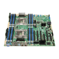
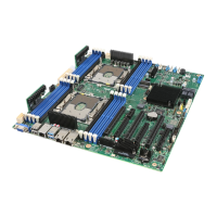
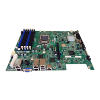
Figure 1. Intel
®
Server Board S2600CW2SR and S2600CWTSR ................................................................. 5
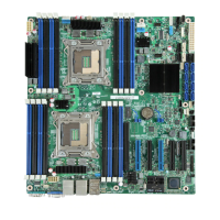
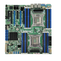
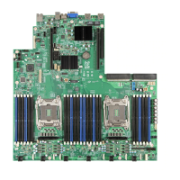
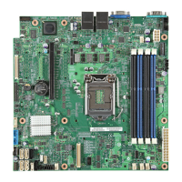
Figure 2. Intel
®
Server Board S2600CW2R and S2600CWTR ...................................................................... 6
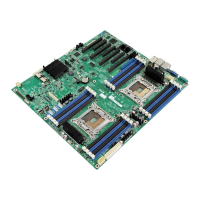
Figure 3. Connector and Component Layout ..................................................................................................... 7
Figure 4. Mounting Hole Locations (1 of 2) ......................................................................................................... 8
Figure 5. Mounting Hole Locations (2 of 2) ......................................................................................................... 9
Figure 6. Major Connector Pin-1 Locations (1 of 2) ...................................................................................... 10
Figure 7. Major Connector Pin-1 Locations (2 of 2) ...................................................................................... 11
Figure 8. Primary Side Card-Side Keep-out Zone ......................................................................................... 12
Figure 9. Second Side Keep-out Zone ................................................................................................................ 13
Figure 10. Rear I/O Layout of Intel
®
Server Board S2600CW .................................................................... 14
Figure 11. Intel
®
Server Board S2600CW2R/S2600CWTR Functional Block Diagram ................... 15
Figure 12. Intel
®
Server Board S2600CW2SR/S2600CWTSR Functional Block Diagram ............. 16
Figure 13. Processor Socket Assembly .............................................................................................................. 17
Figure 14. Memory Subsystem for Intel
®
Server Board S2600CW ......................................................... 24
Figure 15. Intel
®
Server Board S2600CW DIMM Slot Layout..................................................................... 27
Figure 16. BIOS Setup Utility – Video Configuration Options .................................................................. 49
Figure 17. TPM Module ............................................................................................................................................. 51
Figure 18. High-level Fan Speed Control Process ......................................................................................... 80
Figure 19. Intel
®
RMM4 Lite Activation Key Location .................................................................................... 89
Figure 20. Video Connector Pin-out ................................................................................................................ 107
Figure 21. Jumper Blocks ..................................................................................................................................... 111
Figure 22. 5-volt Stand-by Status LED Location ......................................................................................... 116
Figure 23. Fan Fault LED’s Location ................................................................................................................. 117
Figure 24. DIMM Fault LED’s Location ............................................................................................................. 118
Figure 25. Location of System Status, System ID, and POST Code Diagnostic LEDs .................. 119
Figure 26. 750-W Power Supply Outline Drawing ..................................................................................... 122
Figure 27. Differential Noise Test Setup ......................................................................................................... 130
Figure 28. Turn On/Off Timing (Power Supply Signals) ........................................................................... 131
Figure 29. PSON# Required Signal Characteristic ...................................................................................... 133
Figure 30. Outline Drawing .................................................................................................................................. 136
Figure 31. Airflow Diagram ................................................................................................................................... 137
Figure 32. Differential Noise Test Setup ......................................................................................................... 146
Figure 33. POST Code Diagnostic LED Decoder ......................................................................................... 176