3-66 Keysight B1505A User’s Guide, Edition 12
Accessories
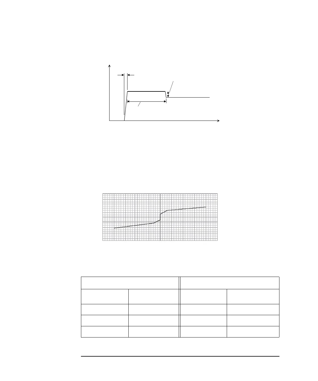
Figure 3-23 Transient Response
I-V Characteristics of N1267A
The N1267A has the I-V characteristics due to the internal semiconductor switches
shown in Figure 3-21. When the device ON state characteristics is monitored, the
voltage actually applied to the DUT will be the HCSMU setting voltage minus the
voltage drop shown below. The voltage drop value varies by the current.
Figure 3-24 HCSMU Output Current vs Voltage Drop
Table 3-18 Voltage Drop
Time
Current limit change
Current limit period =
HVSMU current behavior
Transition time (OFF to ON) = minimum 20 Ms
OFF
ON
maximum 4 mA (1500 V to 3000 V)
maximum 8 mA (up to 1500V)
HVSMU output voltage x 2.5 Ms (at 4 mA compliance)
HVSMU output voltage x 5 Ms (at 8 mA compliance)
Transistor measurement Diode measurement
Voltage drop
Current I
0
a
a. I
0
: HCSMU output current (A)
Voltage drop
Current I
0
a
20 I
0
|I
0
| 30 mA 58 I
0
|I
0
| 10 mA
0.6 + 0.27 I
0
30 mA < |I
0
| 3 A 0.6 + 0.24 I
0
10 mA < |I
0
| 3 A
1.3 + 0.043 I
0
3 A < |I
0
| 20 A 1.1 + 0.062 I
0
3 A < |I
0
| 20 A
-5.0
-3.0
-1.0
1.0
3.0
5.0
-25.0
-20.0
-15.0
-10.0
-5.0
0.0
5.0
10.0
15.0
20.0
25.0
Vdrop: Voltage drop
I : HCSMU output current
0
0