MT7620 PROGRAMMING GUIDE
Integrated 802.11n MAC/BBP and 2.4 GHz RF/FEM Router-on-a-Chip
MT7620 Overview
The MT7620 SoC includes a high performance 580 MHz MIPS24KEc CPU core and USB host controller/PHY,
which is designed to enable a multitude of high performance, cost-effective IEEE 802.11n applications with a
MediaTek (Ralink) client card.
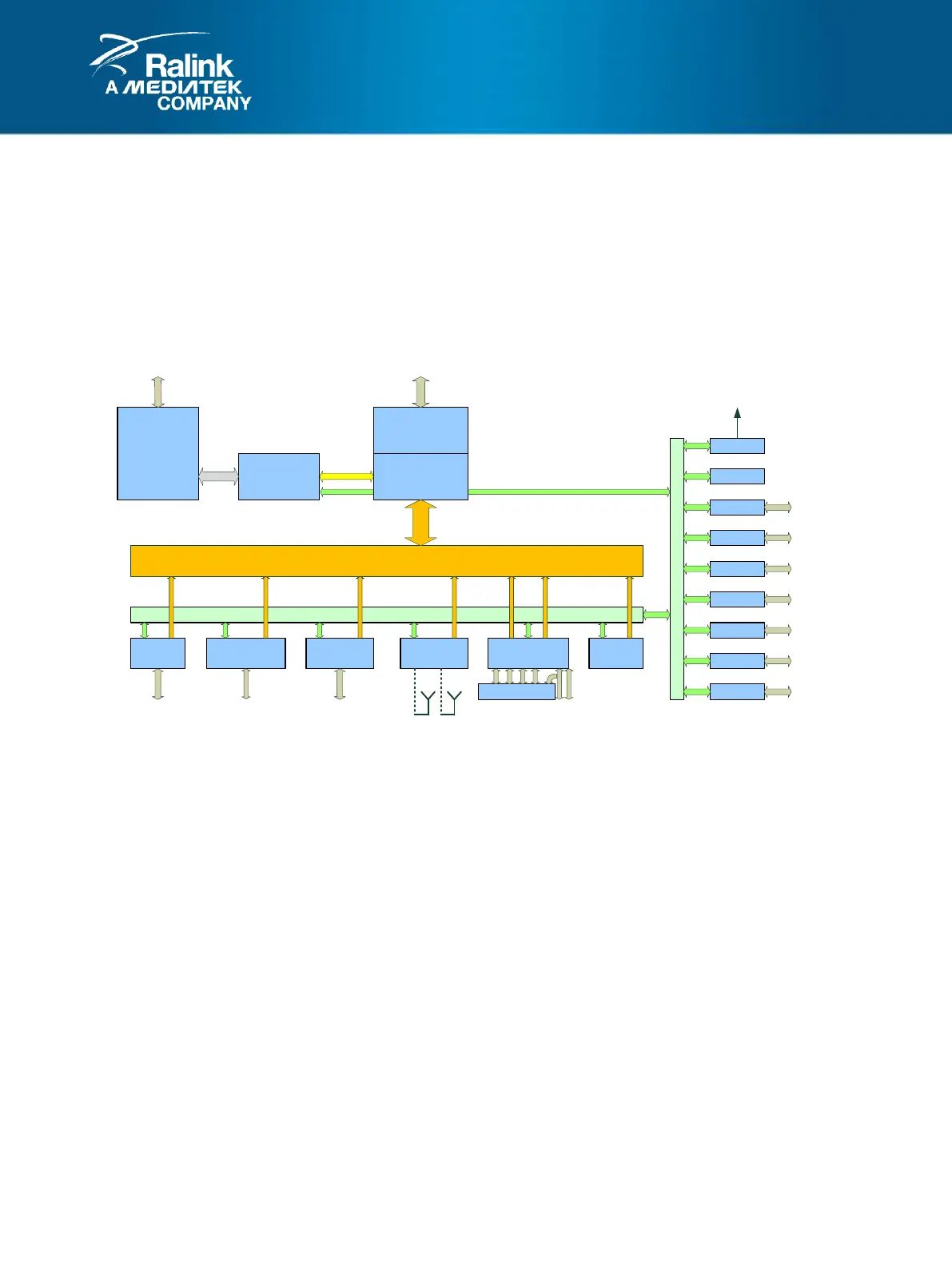
Functional Block Diagram
MIPS 24KEc
64 KB I-Cache
32 KB D-
Cache
(580 MHz)
OCP Bridge
OCP
_IF
Arbiter
DRAM
Controller
RBUS (SYS_CLK)
SPI
NFC
PBUS
GDMA
RJ45 x5
Switch
(4FE + 2GE)
5-Port EPHY
RGMII
TMII/MII
x2
PCIe 1.1
PHY
Single-Port
USB 2.0 PHY
Host/
Device
PCIe x1
UART
GPIO
PCM x4
I2S
I2C
I2S
PBUS
INTC
I2C
GPIO
/LED
SPI
NAND
UART
To CPU
interrupt
s
16-Bit
SDR/DDR1/DDR2
EJTAG
WLAN
11n 2x2
2.4 GHz
Timer
PCM
SDHC
SD
Figure 1-1 MT7620 Block Diagram
There are several masters (MIPS 24KEc, USB , PCI Express) in the MT7620 SoC on a high performance, low
latency Rbus, (Ralink Bus). In addition, the MT7620 SoC supports lower speed peripherals such as UART, GPIO,
and SPI via a low speed peripheral bus (Pbus). The SDRAM/DDR1/DDR2 controller is the only bus slave on the
Rbus. It includes an Advanced Memory Scheduler to arbitrate the requests from bus masters, enhancing the
performance of memory access intensive tasks.