MT7620 PROGRAMMING GUIDE
Integrated 802.11n MAC/BBP and 2.4 GHz RF/FEM Router-on-a-Chip
2.15 Memory Controller
2.15.1 Features
1 SDRAM/DDR2 (16 b) chip selection
128 MB (SDRAM)/128 MB (DDR1)/256 MB (DDR2) per chip selection
SDRAM transaction overlapping by early active and hidden pre-charge
User SDRAM Init commands
4 banks per SDRAM chip select
SDRAM burst length: 4 (fixed)
DDR2 burst length: 4/8 (programmable)
Wrap-4 transfer
Bank-Raw-Column and Raw-Bank-Column address mapping
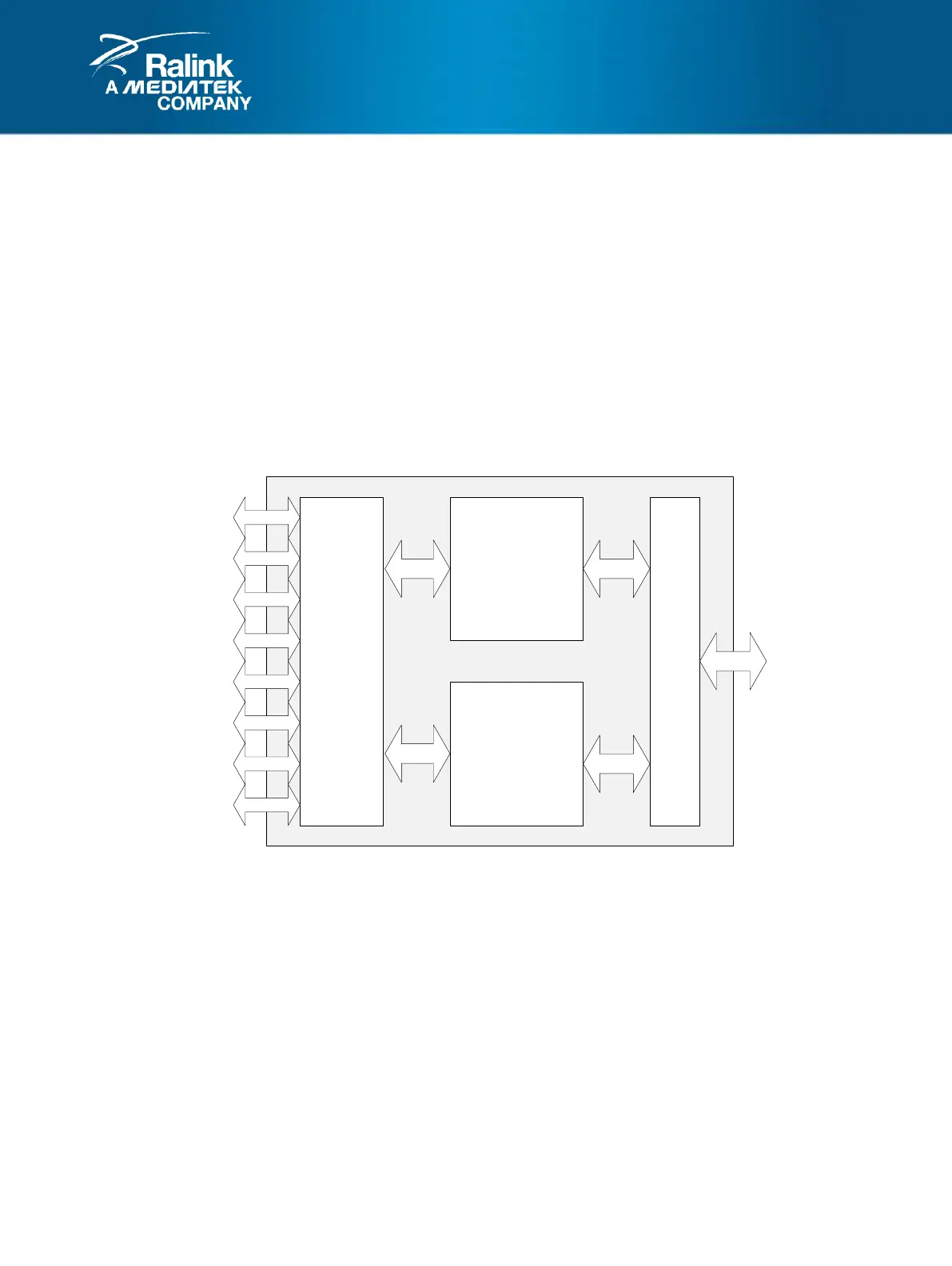
2.15.2 Block Diagram
SDRAM Controller
DDR2 Controller
PIN
Mux
Scheduler
External I/O
Pins
From Bus
Masters
Figure 2-16 SRAM/SDRAM Controller Block Diagram
2.15.3 SDRAM Initialization Sequence
SDRAMs require an initialization sequence before they are ready for reading and writing. The initialization
sequence is described below.
1. Set SDRAM related timing in SDRAM_CFG0.
2. Set SDRAM size and refresh time in SDRAM_CFG1 register with SDRAM_INIT_START = 1.
3. Read SDRAM_INIT_DONE in SDRAM_CFG1 register.
4. If SDRAM_INIT_DONE !=1, go to step 3, else the SDRAM initialization sequence is finished.


 To Next Page