MT7620 PROGRAMMING GUIDE
Integrated 802.11n MAC/BBP and 2.4 GHz RF/FEM Router-on-a-Chip
2.11 PCM Controller
2.11.1 Features
PCM module provides PBUS interface for register configuration and data transfer
Two clock sources are reserved for PCM circuit. (From internal clock generator, INT_PCM_CLK and
EXT_PCM_CLK)
PCM module can drive a clock out (with fraction-N dividor) to an external codec.
Up to 4 channels PCM are available. 4 to 128 slots are configurable.
Each channel supports a-law (8-bit)/u-law (8-bit)/raw-PCM (8-bit and 16-bit) transfer.
Hardware converter of a-law<->raw-16 and u-law <-> raw-16 are implemented in design.
Support long (8 cycle)/short (1 cycle)/configurable (intervals are configurable, use to emulate I
2
S
interface) FSYNC.
DATA & FSYNC can be driven and sampled by either rising/falling of clock.
Last bit of DTX can be configured as tri-stated on falling edge.
Beginning of each slot is configurable by 10-bit registers on each channel.
32-byte FIFO are available for each channel
PCM interface can emulate I2S interface (only 16-bit data-width supported ).
MSB/LSB order is configurable.
Supports both a-law/u-law (8-bits) linear PCM(16-bit) and linear PCM(16-bit) a-law/u-law (8-bit)
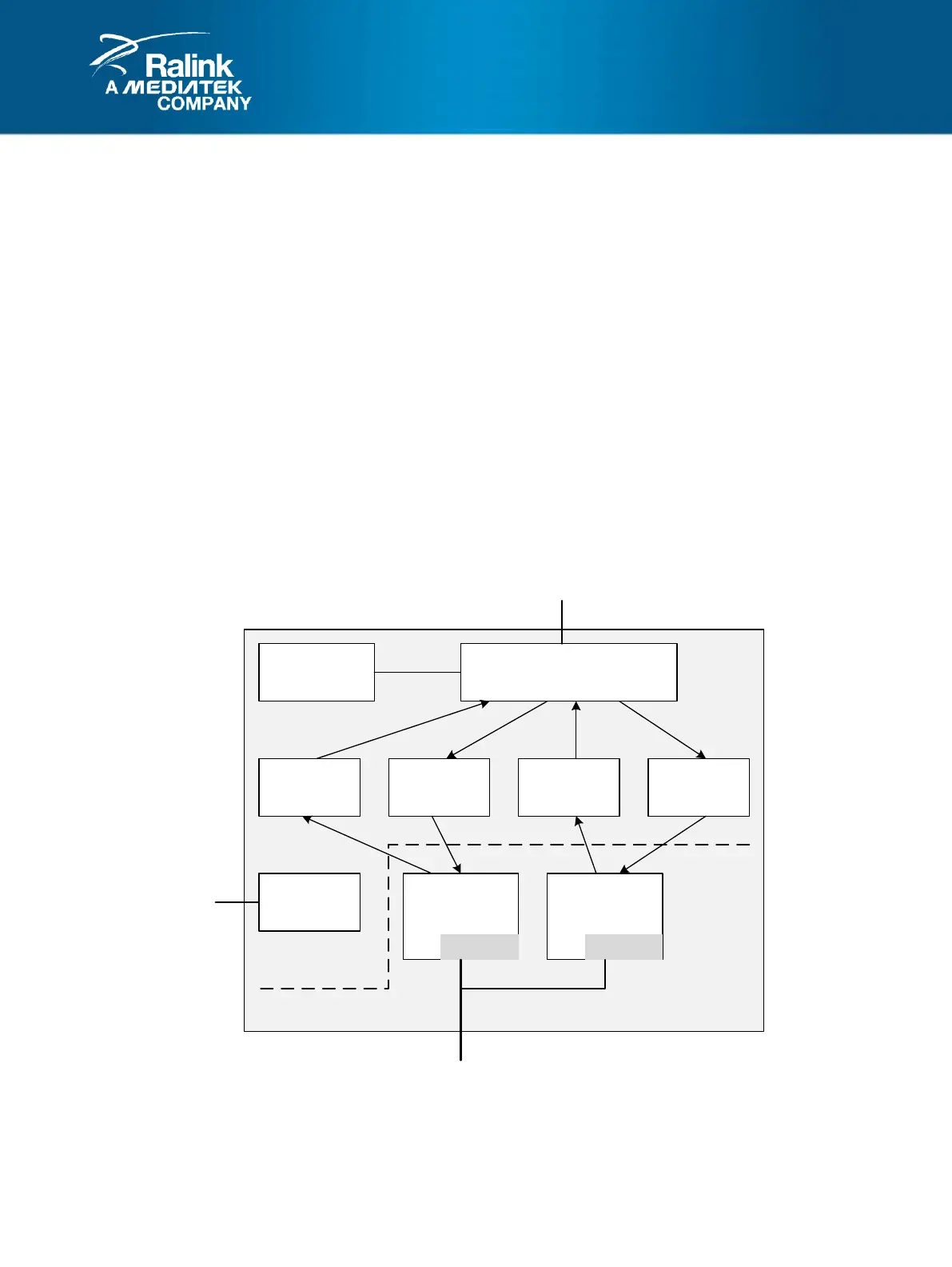
2.11.2 Block Diagram
PCM Control
Status Register
PBUS LTF
RFIFO
(32 bytes)
TFIFO
(32 bytes)
RFIFO
(32 bytes)
TFIFO
(32 bytes)
GDMA LTF
CH1 CH0
a/ulawa/ulaw
PBUS
PCM Module
PCM IF/I2S
IF
PCM clock domain
SYS clock domain
DRAM
Figure 2-11 PCM Controller Block Diagram