M800S/M80/E80 Series Connection and Setup Manual
4 General Specifications
107
IB-1501269-J
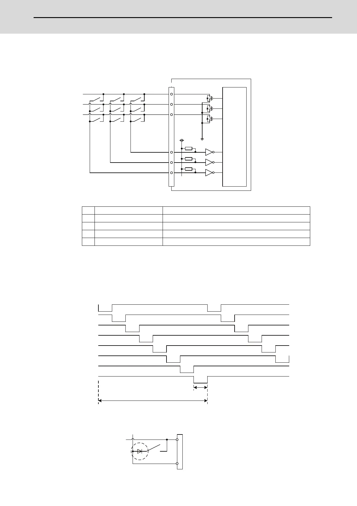
(a) Outline of scan input circuit
Input circuit
Input conditions
(*1) Note that "11.68 ms or more" is a guide of the "Input signal holding time". The input signal is
recognized only when its "ON" state is held longer than the ladder processing cycle time.
The common signals are changed over with scan input as shown in the following drawing. Key input data
can be received when the common signal is LOW.
The common signal changeover cycle is 11.68ms, but the input signal will not be recognized unless it is
held for the ladder processing cycle time or longer.
(Note) To perform a scan input, connect a sneak path prevention diode as illustrated below.
Input signals may not be read correctly without the sneak path prevention diode.
1 Number of points 64 points
2 Configuration Matrix of 8 common signals × 8 data signals
3 Rated voltage 5 VDC
4 Minimum applicable load 1.4 mA per point
5 Input signal holding time 11.68 ms or more (*1)
OPKB
0V
:
:
KYC0*
KYC1*
KYC2*
:
:
5V
:
:
:
:
KYD0*
KYD1*
KYD2*
:
:
Control
circuit
KYC0*
KYC1*
KYC2*
KYC3*
KYC4*
KYC5*
KYC6*
KYC7*
11.68ms
1.46ms
KYC0* - KYC7*
KYD0* - KYD7*
Sneak path
prevention diode
 Loading...