419
CHAPTER 18 SERIAL INTERFACE CHANNEL 1
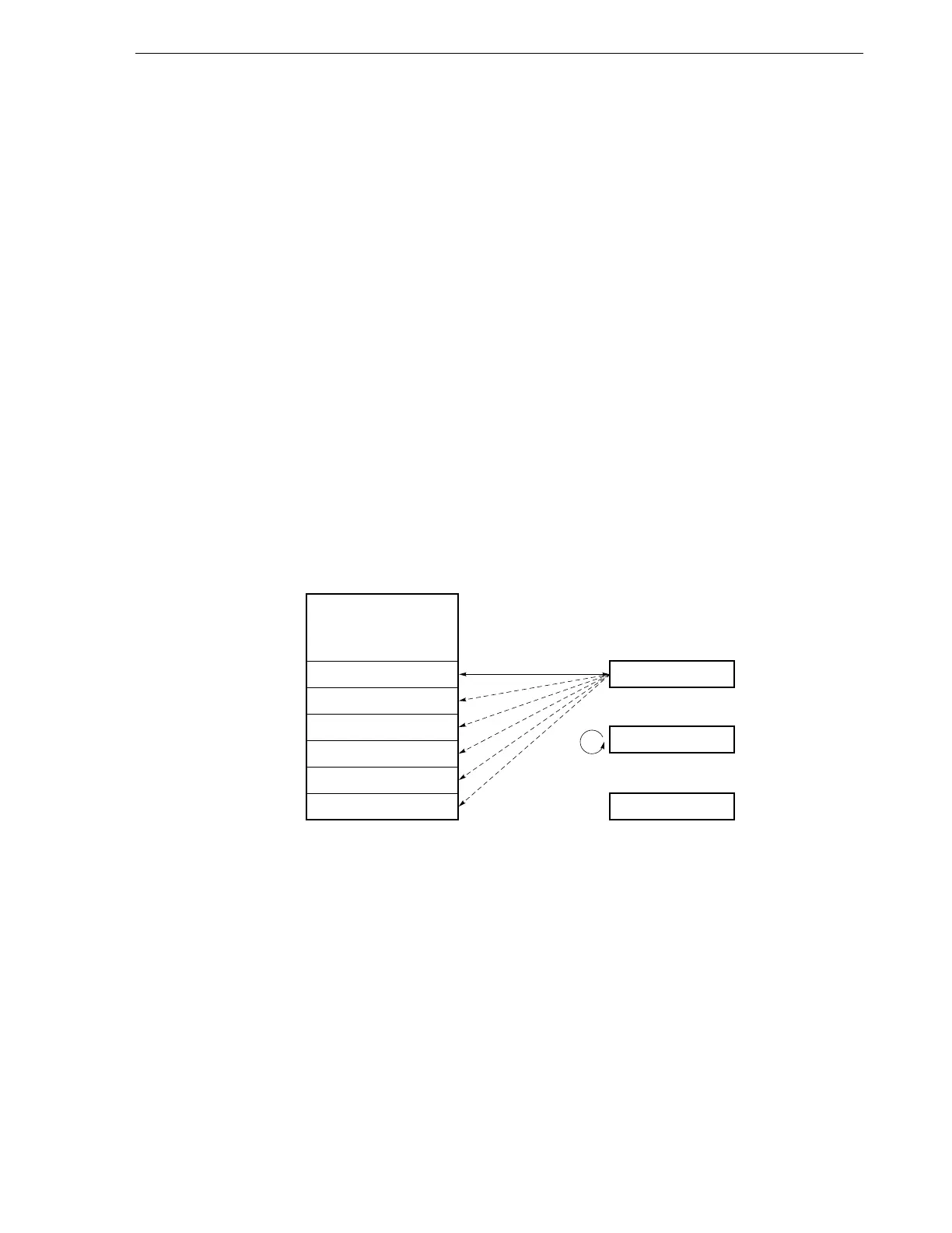
In 6-byte transmission/reception (ARLD=0, RE=1) in basic transmit/receive mode, buffer RAM operates as follows.
(i) Before transmission/reception (Refer to Figure 18-10 (a))
After any data has been written to serial I/O shift register 1 (SIO1) (start trigger: this data is not
transferred), transmit data 1 (T1) is transferred from the buffer RAM to SIO1. When transmission
of the first byte is completed, the receive data 1 (R1) is transferred from SIO1 to the buffer RAM, and
automatic data transmit/receive address pointer (ADTP) is decremented. Then transmit data 2 (T2)
is transferred from the buffer RAM to SIO1.
(ii) 4th byte transmission/reception point (Refer to Figure 18-10 (b))
Transmission/reception of the third byte is completed, and transmit data 4 (T4) is transferred from
the buffer RAM to SIO1. When transmission of the fourth byte is completed, the receive data 4 (R4)
is transferred from SIO1 to the buffer RAM, and ADTP is decremented.
(iii) Completion of transmission/reception (Refer to Figure 18-10 (c))
When transmission of the sixth byte is completed, the receive data 6 (R6) is transferred from SIO1
to the buffer RAM, and the interrupt request flag (CSIIF1) is set (INTCSI1 generation).
Figure 18-10. Buffer RAM Operation in 6-Byte Transmission/Reception
(in Basic Transmit/Receive Mode) (1/2)
(a) Before transmission/reception
Transmit data 1 (T1)
Transmit data 2 (T2)
Transmit data 3 (T3)
Transmit data 4 (T4)
Transmit data 5 (T5)
Transmit data 6 (T6)
FADFH
FAC5H
FAC0H
Receive data 1 (R1) SIO1
0 CSIIF1
5 ADTP
–1