44
Specifications Section 2-1
Transistor Outputs (Sinking or Sourcing)
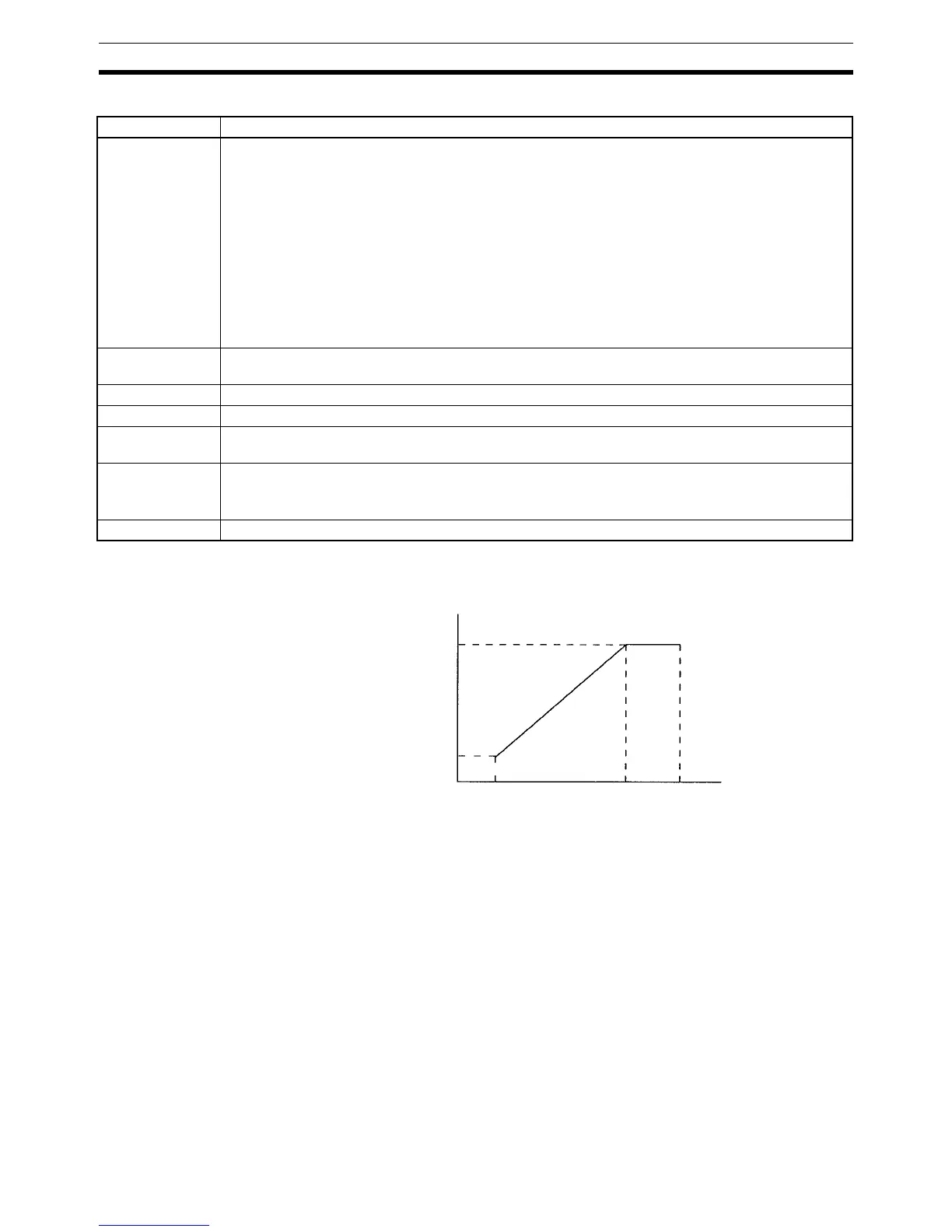
Note The following graph shows the maximum switching capacity.
!Caution Do not apply voltage in excess of the maximum switching capacity to an out-
put terminal. It may result in damage to the product or fire.
Item Specification
Max. switching
capacity (See
note.)
CPU Units with 10 or 20 I/O Points
OUT01000 to OUT01007:40 mA/4.5 VDC to 300 mA/20.4 VDC, 300 mA (20.4 VDC to 26.4 VDC)
CPU Units with 32 I/O Points
OUT01000 to OUT01007:40 mA/4.5 VDC to 300 mA/20.4 VDC, 300 mA (20.4 VDC to 26.4 VDC)
OUT01100 to OUT01107:40 mA/4.5 VDC to 100 mA/20.4 VDC, 100 mA (20.4 VDC to 26.4 VDC)
Expansion I/O Units
OUT01@00 to OUT01@07:40 mA/4.5 VDC to 300 mA/20.4 VDC, 300 mA (20.4 VDC to 26.4 VDC)
OUT01@08 to OUT01@15:40 mA/4.5 VDC to 100 mA/20.4 VDC, 100 mA (20.4 VDC to 26.4 VDC)
When using OUT01000 or OUT01001 as a pulse output, connect a dummy resistor as required to
bring the load current between 10 and 150 mA. If the load current is below 10 mA, the ON/OFF
response time will be longer and high-speed pulses will not be output.
The transistor will heat if used at 150 mA or higher, possibly damaging elements.
Max. inrush cur-
rent
0.9 A for 10 ms (charging and discharging waveform)
Leakage current 0.1 mA max.
Residual voltage 0.8 V max.
ON delay OUT01000 and OUT01001: 20 µs max.
OUT01002 and up: 0.1 ms max.
OFF delay OUT01000 and OUT01001: 40 µs max. at 10 to 300 mA
0.1 ms max. at 0.5 to 10 mA
OUT01002 and up: 1 ms max. at 0.5 mA or more
Fuse 1 fuse for each 2outputs (cannot be replaced by user)
Output
current
(mA)
Output
voltage