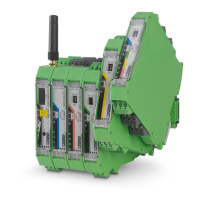
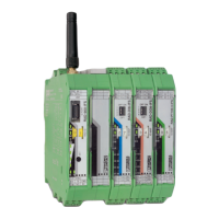
RAD-900-...
46/138
PHOENIX CONTACT 3827_en_B
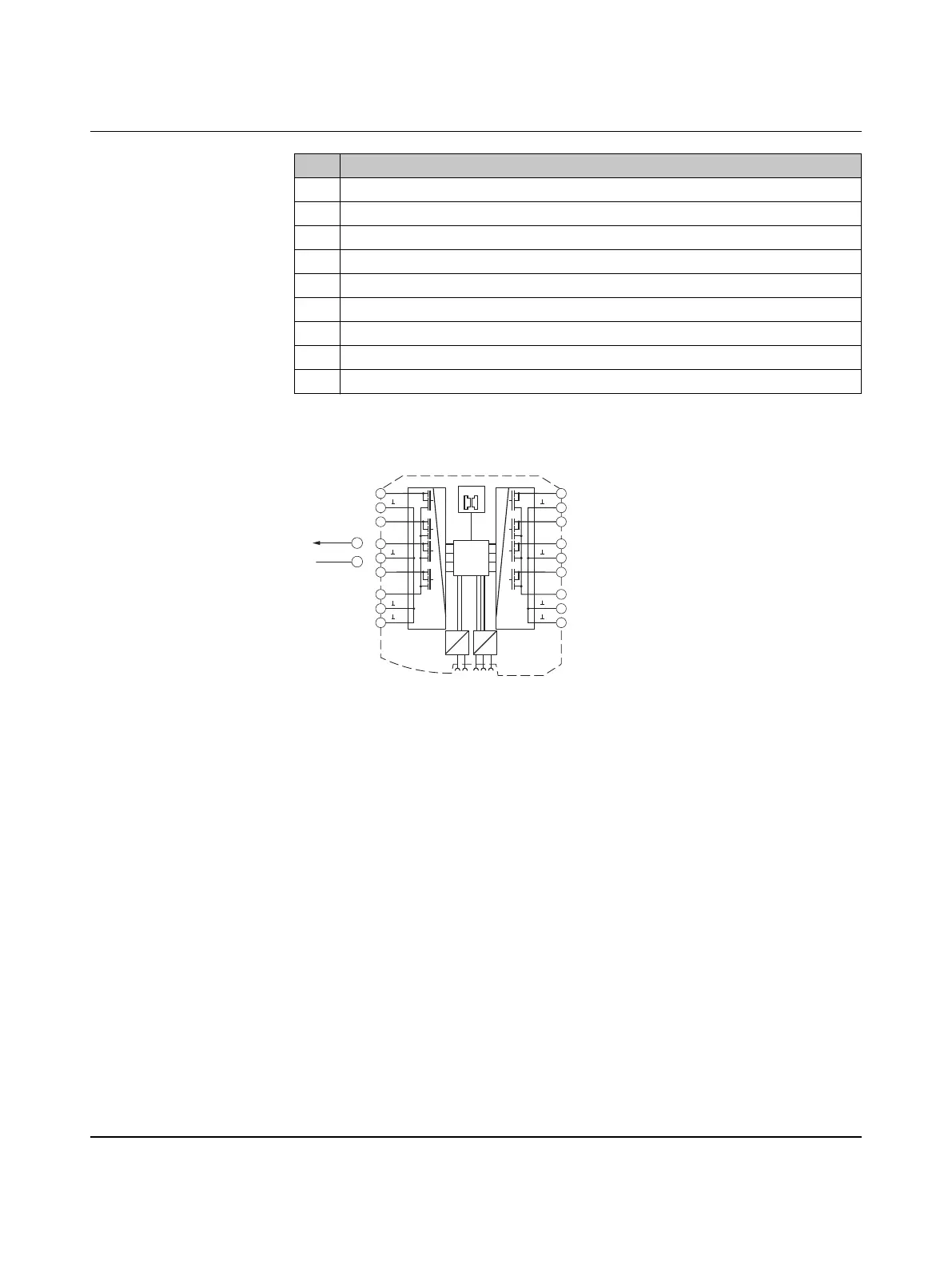
3.7.2 Basic circuit diagram
Figure 3-33 Basic circuit diagram for the RAD-DO8-IFS
3.7.3 Setting the DIP switches
You can use the DIP switches on the front to set the behavior of the outputs in the event of
an error (e.g., interruption of the wireless connection). Any changes in the setting of the DIP
switches will be directly applied.
– RESET = Output value is set to 0
– HOLD = Hold last output value
7 DIN rail
8 Metal foot catch for DIN rail fixing
9 Transistor outputs 5 + 6
10 Transistor outputs 7 + 8
11 Supply voltage for outputs 5 ... 8
12 Status LEDs of transistor outputs DO1 ... DO8
13 ERR status LED, red (communication error)
14 DAT status LED, green (bus communication)
15 PWR status LED, green (supply voltage)
Item Designation
30,5 V DC
2.1
2.2
GND
µC
1.1
1.2
1.3
2.1
2.2
2.3
3.1
3.2
3.3
6.1
6.2
6.3
5.1
5.2
5.3
4.1
4.2
4.3
IO-MAP
0
1
DC
DC
IFS
IFS
DO
2
DO
4
DO
1
DO
3
Do
8
DO
6
Do
7
DO
5
+24V
1-4
+24V
5-8
1-4
1-4
1-4
1-4
5-8
5-8
5-8
5-8
 Loading...