Programmable I/O Ports
M30240 Group
Rev.1.00 Sep 24, 2003 Page 116 of 360
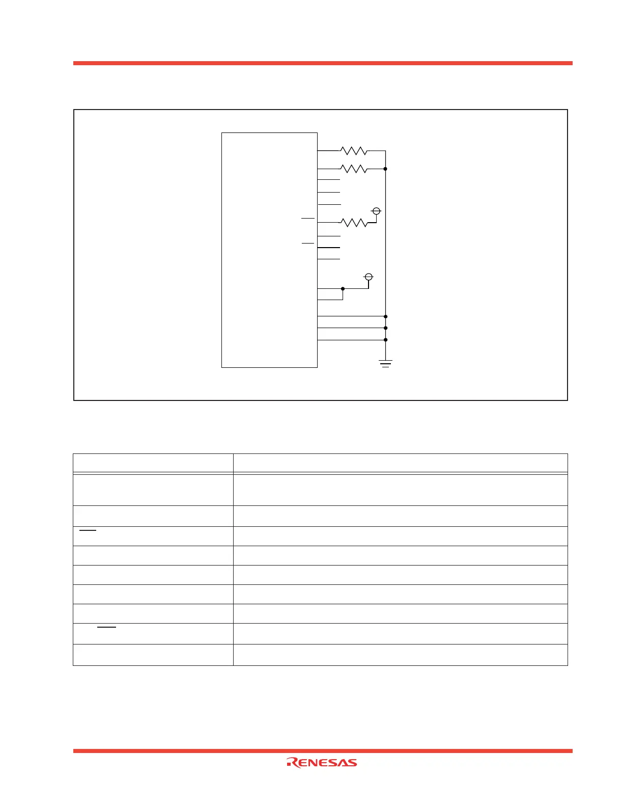
Figure 1.113: Example connection unused pins
Table 1.36: Example connection of unused pins in single-chip mode
Pin name Connection
Ports P0 to P3, P6 to P8, P10
(excluding P8
3
, P8
5
, P8
6
)
After setting for input mode, connect every pin to Vss or Vcc via a resistor; or
after setting for output mode, leave these pins open
X
OUT
Open (When using external clock)
NMI Connect via resistor to Vcc (pull-up)
AVcc Connect to Vcc
Avss, Vref, BYTE Connect to Vss
USB D+, USB D- Open
EXTCAP Connect to Vcc (when DC-DC converter is disabled)
P8
6
/SOF
After setting for output mode in normal operation, leave this pin open
P8
3
/ATTACH
After setting for output mode in normal operation, leave this pin open
Port P0 to P3, P6-P8, P10
(except P8
3
, P8
5
, P8
6
)
(Input mode)
·
·
·
(Input mode)
(Output mode)
USB D+
USB D-
Microcomputer
AV CC
EXTCAP (Note 1)
VCC
XOUT
P8
6
/SOF
P8
3
/ATTACH
Open
BYTE
AV
SS
VREF
VSS
Open
NMI
·
·
·
Open
Open
Open
Open
Note: This is an example when the DC-DC converter is disabled
 Loading...


