Frequency Synthesizer
M30240 Group
Rev.1.00 Sep 24, 2003 Page 291 of 360
(5) After waiting the time required for supplying approximately 3.3V to the EXTCAP terminal, the USB
clock enable bit should be set to “1.” The wait time then is (C+1)ms (the C is the capacity (
µF) of the
condenser that is connected to the EXTCAP terminal).
(6) After enabling the USB clock and waiting four cycles of the
φ or greater, the USB enable bit should
be set to “1.”
3.1.4.3 Prescaler
Clock f(X
IN) is prescaled down by the frequency synthesizer prescaler register (FSP) to generate fPIN.
When the frequency synthesizer prescaler register is set at 255, the prescaler is disabled and f
PIN =
f(X
IN). Table 3.2 shows some examples of how the frequency synthesizer prescaler register is set.
f
PIN = f(XIN) / 2(n+1) n: FSP value Note: The value of f
PIN
should not be set below 1 MHz.
3.1.4.4 Frequency Multiplier
Clock fVCO is a multiplied version of clock fPIN. fVCO is generated via the Frequency Synthesizer Mul-
tiply register (FSM). When the Frequency Multiply register is set to 255, multiplication is disabled and
f
VCO = fPIN. The value of n should be set so that fVCO becomes 48MHz. Table 3.3 shows some exam-
ples of how the frequency synthesizer multiply register is set.
f
VCO = fPIN X 2(n+1) n: FSM value
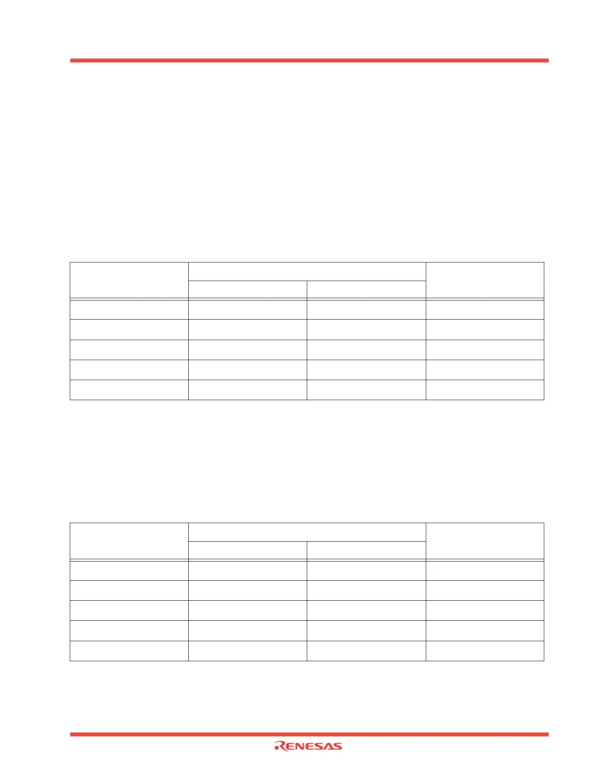
Table 3.3: Example of Setting the Frequency Multiply Register (FSM)
Table 3.2: Example of Setting the Frequency Synthesizer Prescaler Register (FSP)
f
PIN
FSP
f(X
IN)
Decimal List Hexadecimal List
12 MHz
255
FF
16
12.00 MHz
1 MHz
5
05
16
12.00 MHz
2 MHz
2
02
16
12.00 MHz
3 MHz
1
01
16
12.00 MHz
6 MHz
0
00
16
12.00 MHz
fPIN
FSM
fVCO
Decimal List Hexadecimal List
1 MHz
33
4A
16
48.00 MHz
2 MHz
11
0B
16
48.00 MHz
4 MHz
5
05
16
48.00 MHz
6 MHz
3
03
16
48.00 MHz
12 MHz
1
01
16
48.00 MHz
 Loading...


