Processor Mode
M30240 Group
Rev.1.00 Sep 24, 2003 Page 13 of 360
1.2.2 Processor Mode
Figure 1.7 shows the processor mode registers 0 and 1.
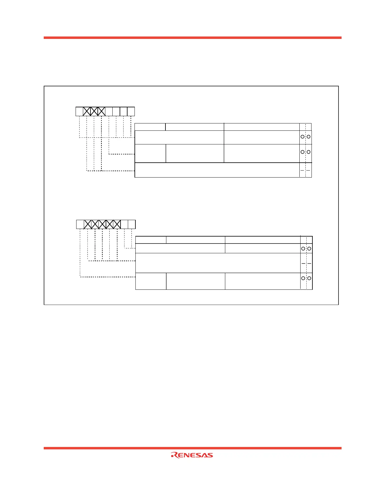
Figure 1.7: Processor mode registers 0 and 1
Processor mode register 0 (Note
)
Symbol Address When reset
PM0 0004
16 0016 (Note)
Bit name FunctionBit symbol
WR
b7 b6 b5 b4 b3 b2 b1 b0
Reserved bit
Note : Set bit 1 of the protect register (address 000A
16) to “1” when writing new
values to this register.
Processor mode register 1 (Note)
Symbol Address When reset
PM1 0005
16 00XXXXX02
Bit name FunctionBit symbol
WR
b7 b6 b5 b4 b3 b2 b1 b0
Nothing is assigned.
These bits can neither be set nor reset. When read, their contents are
indeterminate.
Reserved bit
Must always be set to “0”
0
Note : Set bit 1 of the protect register (address 000A
16) to “1” when writing new values
to this register.
PM17
Wait bit
0 : No wait state
1 : Wait state inserted
Must always be set to "0"
PM03
Software reset bit
The device is reset when this bit is set
to “1”. The value of this bit is “0” when
read.
Nothing is assigned. These bits can neither be set nor reset. When read,
their contents are indeterminate.
0
0000
0
 Loading...


