Frequency Synthesizer
M30240 Group
Rev.1.00 Sep 24, 2003 Page 290 of 360
Figure 3.5: Frequency Synthesizer Multiply Register (FSM)
Figure 3.6: Frequency Synthesizer Divide Register (FSD)
3.1.3 Operation
The frequency synthesizer consists of a prescaler, frequency multiplier macro, a frequency divider
macro, and five registers, namely FSP, FSM, FSC, FSD, and FSCCR. Clock f(X
IN
) is prescaled down
using FSP to generate f
PIN
. f
PIN
is multiplied using FSM to generate an f
VCO
clock which is then divided
using FSD to produce the clock f
SYN
. The f
VCO
clock is optimized for 48 MHz operation and is buffered
and sent out of the frequency synthesizer block as signal f
USB
. This signal is used by the USB block.
3.1.4 Frequency Synthesizer Interface
3.1.4.1 Precautions
When using the frequency synthesizer control register, connect a low pass filter to the LPF terminal.
When the frequency synthesizer is enabled, do not use the output of the frequency synthesizer until after
a 2~5ms delay. That will stabilize the output. Also, after the frequency synthesizer has been enabled,
because the output is temporarily (2-5ms) unstable, the contents of none of the registers should be
changed.
3.1.4.2 Setup after Hardware Reset
(1) After canceling the protect and setting the frequency synthesizer related registers (03DB
16
to 3DE
16
address numbers), the frequency synthesizer should be enabled.
(2) The protect register should be set to write disabled. A 2.2ms wait is necessary.
(3) The frequency synthesizer locked status bit should be checked. It is necessary to recheck after a
wait of 0.1ms if it is “0”.
(4) If using the DC-DC converter built into the USB, the USB line driver supply selection bit of the USB
control register should be set to “1.” At that time, the USB line driver drive ability selection bit should be
set to “0.” In the normal mode, the USB line driver drive ability selection bit should be kept at “0.” It should
be “1” when in the suspend mode.
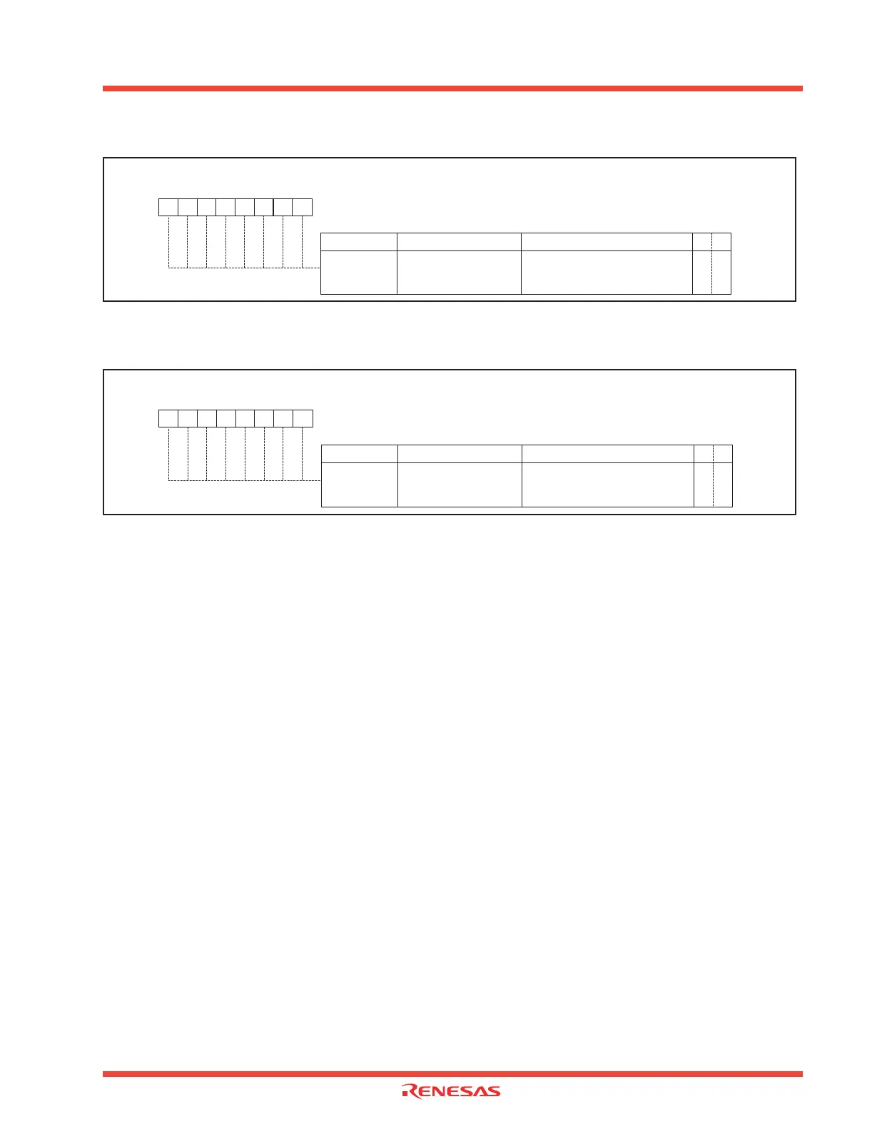
Bit Symbol Bit Name Function R W
FSM
Frequency Synthesizer
Multiplier Value
O O
Symbol
FSM
Address
03DD
16
When reset
FF
16
Frequency Synthesizer Multiply Register
b7 b5b6 b4 b3 b2 b1 b0
Generates f
VCO
by multiplying f
PIN
f
VCO
= f
PIN
X 2(n + 1)
n: FSM value
Bit Symbol Bit Name Function R W
FSD
Frequency Synthesizer
Divider Value
O O
Symbol
FSD
Address
03DF
16
When reset
FF
16
Frequency Synthesizer Divide Register
b7 b5b6 b4 b3 b2 b1 b0
Generates f
SYN
by dividing f
VCO
f
SYN
= f
VCO
/ 2(m + 1)
m: FSD value
 Loading...


