Frequency Synthesizer
M30240 Group
Rev.1.00 Sep 24, 2003 Page 289 of 360
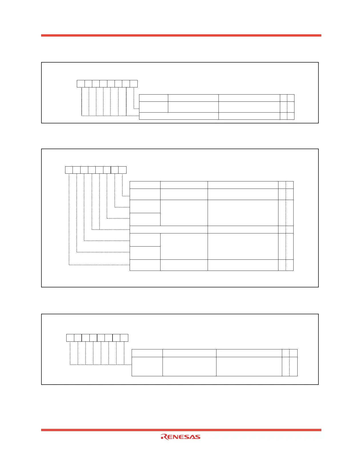
Figure 3.2: Frequency Synthesizer Clock Control Register (FSCCR)
Figure 3.3: Frequency Synthesizer Related Register (FSC)
Figure 3.4: Frequency Synthesizer Prescaler Register (FSP)
Bit Symbol Bit Name Function R W
FSCCR0
Reserved
Clock source selection
0 : Xin
1 : fsyn
Must always be set to "0"
O O
O O
O O O O O O O
Symbol
FSCCR
Address
03DB
16
When reset
00
16
Frequency Synthesizer Clock Control Register
b7 b5b6 b4 b3 b2 b1 b0
Bit Symbol Bit Name Function R W
FSE
Reserved
Frequency Synthesizer
Enable
0 : Disabled
1 : Enabled
Must always be set to "0"
O O
O O
O O
Symbol
FSC
Address
03DC
16
When reset
60
16
Frequency Synthesizer Control Register
b7 b5b6 b4 b3 b2 b1 b0
VCO0
VCO1
VCO Gain Control
Bit 2 Bit 1
0 0: Lowest Gain (Note)
0 1: Low Gain
1 0: High Gain
1 1: Highest Gain
O O
Bit 6 Bit 5
0 0: Disabled
0 1: Low Current
1 0: Intermediate Current (Note)
1 1: High Current
O O
CHG0
CHG1
LS
O O
LPF Current Control
Frequency Synthesizer
Lock Status
0 : Unlocked
1 : Locked
Note: Recommended
Bit Symbol Bit Name Function R W
FSP
Frequency Synthesizer
Prescaler Value
O O
Symbol
FSP
Address
03DE
16
When reset
FF
16
Frequency Synthesizer Prescaler Register
b7 b5b6 b4 b3 b2 b1 b0
Generates f
PIN
f
PIN
=f(Xin) / 2(n + 1)
n: FSP value
 Loading...


