A-D Converter
M30240 Group
Rev.1.00 Sep 24, 2003 Page 253 of 360
2.6.7 Sensor Output Impedance
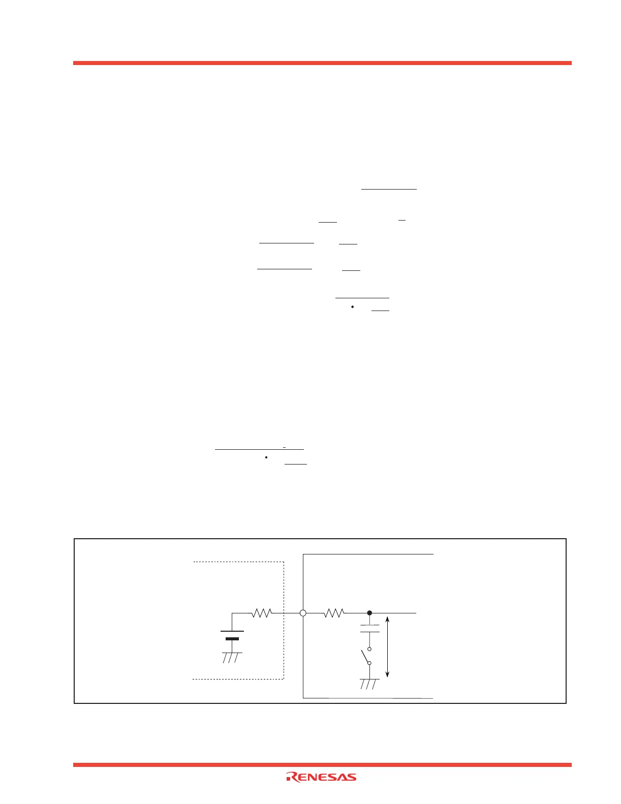
To carry out A-D conversion properly, charging the internal capacitor C shown in Figure 2.99 has to be
completed within a specified period of time. With T as the specified time, time T is the time that switches
SW2 and SW3 are connected to O in Figure 2.98. Let output impedance of sensor equivalent circuit be
R0, microcomputer’s internal resistance be R, precision (error) of the A-D converter be X, and the A-D
converter’s resolution be Y (Y is 1024 in the 10-bit mode, and 256 in the 8-bit mode).
With the model shown in Figure 2.99 as an example, when the difference between V
IN and Vcc becomes
0.1LSB, we find impedance R0 when voltage between pins Vcc changes from 0 to V
IN-(0.1/1024) VIN in
time T. (0.1/1024) means that A-D precision drop due to insufficient capacitor charge is held to 0.1LSB
at time of A-D conversion in the 10-bit mode. Actual error however is the value of absolute precision
added to 0.1LSB. When f(X
IN) = 12 MHz, T = 0.25 µs in the A-D conversion mode with sample & hold.
Output impedance R0 for sufficiently charging capacitor C within time T is determined as follows.
Thus, the allowable output impedance of the sensor circuit capable of thoroughly driving the A-D
converter turns out to be approximately 1.2 kΩ. Tables 2.35 and 2.36 show output impedance values
based on the LSB values.
Figure 2.99: Circuit equivalent to A-D conversion terminal
Vc is generally Vc = V
IN {1 - e
_
And when t = T, Vc = V
IN - VIN = VIN 1 - X
X
Y
C (R0+ R)
T
C (R0 + R)
=
X
Y
e -
T
C (R0 + R)
= In
X
Y
-
Therefore, R0 = -
C In
X
Y
T
- R
Y
)
(
}
T = 0.25 µs, R = 7.8 kΩ, C = 3 pF, X = 0.1, and Y = 1024, Therefore,
R0 = -
0.25 x 10
-6
3.0 x 10
-12
In 0.1
1024
7.8 x 10
3
= 1225
-
VC
C (3.0pF)
V
IN
Microprocessor's inside
Sensor-equivalent circuit
R (7.8kΩ)
R0
 Loading...


