Frequency Synthesizer Circuit
M30240 Group
Rev.1.00 Sep 24, 2003 Page 38 of 360
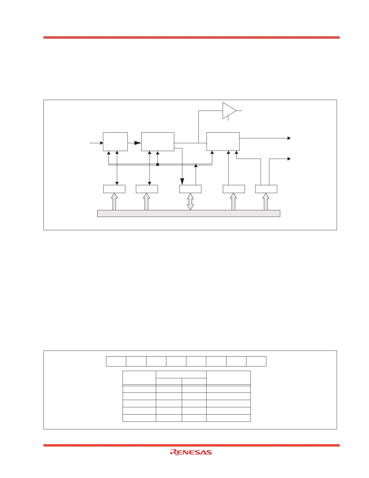
1.2.17 Frequency Synthesizer Circuit
The Frequency Synthesizer Circuit generates a 48MHz clock needed by the USB block and a clock f
SYN
that are both a multiple of the external input reference clock f(X
IN
). A block diagram of the circuit is shown
in Figure 1.23.
Figure 1.23: Frequency Synthesizer Circuit
The frequency synthesizer consists of a prescaler, frequency multiplier macro, a frequency divider
macro, and five registers, namely FSP, FSM, FSC, FSD, and FSCCR. Clock f(X
IN
) is prescaled down
using FSP to generate f
PIN
. f
PIN
is multiplied using FSM to generate an f
VCO
clock which is then divided
using FSD to produce the clock f
SYN
. The f
VCO
clock is optimized for 48 MHz operation and is buffered
and sent out of the frequency synthesizer block as signal f
USB
. This signal is used by the USB block.
1.2.17.1 Prescaler
Clock f
PIN
is a divided down version of clock f(X
IN
) (see Figure 1.24). The relationship between f
PIN
and the clock input to the prescaler f(X
IN
) is as follows:
• f
PIN
= f(X
IN
) / 2(n+1) where n is a decimal number between 0 and 254.
Setting FSP to 255 disables the prescaler and f
PIN
= f(X
IN
).
• Note: f(X
IN
) frequency below 1 MHz is not recommended.
Figure 1.24: Frequency Synthesizer Prescaler Register (FSP)
FSP
Data Bus
FSM FSC FSD
03DE 03DD
03DC 03DF
Frequency
Multiplier
Frequency
Divider
8 Bit
LS
8 Bit
f(X
IN
)
f
VCO
f
SYN
f
USB
Prescaler
8 Bit
f
PIN
FSCCR
FSCCR0
03DB
EN
USBC5
2
f
PIN
FSP
f(Xin)
Dec(n) Hex(n)
12 MHz 255 FF 12.00 MHz
1 MHz 5 05 12.00 MHz
2 MHz 2 02 12.00 MHz
3 MHz 1 01 12.00 MHz
6 MHz 0 00 12.00 MHz
MSB
7
LSB
0
Bit 6 Bit 1 Bit 0
Bit 2
Bit 5 Bit 4 Bit 3Bit 7
Access: R/W
Address: 03DE
16
Reset: FF
16
f(X
IN
)/2(n+1) = f
PIN
 Loading...


