Timer A
M30240 Group
Rev.1.00 Sep 24, 2003 Page 146 of 360
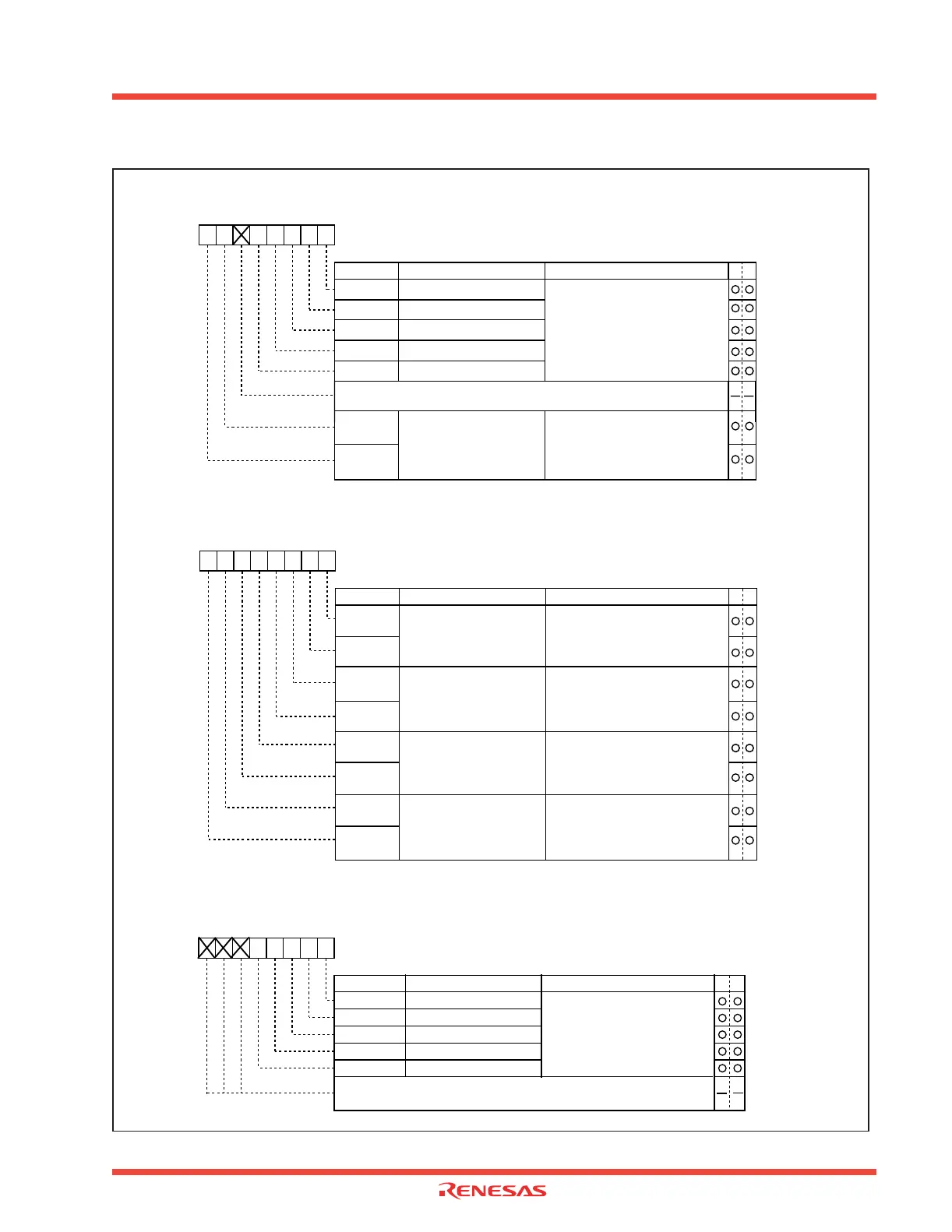
Figure 2.6: Timer A related register (3)
TA1OS
TA2OS
TA0OS
One-shot start flag
Symbol Address When reset
ONSF 0382
16 00X000002
Timer A0 one-shot start flag
Timer A1 one-shot start flag
Timer A2 one-shot start flag
Timer A3 one-shot start flag
Timer A4 one-shot start flag
TA3OS
TA4OS
Bit name FunctionBit symbol
b7 b6 b5 b4 b3 b2 b1 b0
Nothing is assigned.
In an attempt to write to this bit, write “0”. The value, if read, turns out to be indeterminate.
TA0TGL
TA0TGH
0 0 : Input on TA0 IN is selected (Note)
0 1 : TB2 overflow is selected
1 0 : TA4 overflow is selected
1 1 : TA1 overflow is selected
Timer A0 event/trigger
select bit
b7 b6
Note: Set the corresponding port direction register to “0”.
WR
1 : Timer start
When read, the value is “0”
TA1TGL
Symbol Address When reset
TRGSR 038316 0016
Timer A1 event/trigger
select bit
0 0 :
Input on TA1 IN is selected (Note)
0 1 : TB2 overflow is selected
1 0 : TA0 overflow is selected
1 1 : TA2 overflow is selected
Trigger select register
Bit name FunctionBit symbol
b7 b6 b5 b4 b3 b2 b1 b0
0 0 : Input on TA2 IN is selected (Note)
0 1 : TB2 overflow is selected
1 0 : TA1 overflow is selected
1 1 : TA3 overflow is selected
0 0 : Input on TA3 IN is selected (Note)
0 1 : TB2 overflow is selected
1 0 : TA2 overflow is selected
1 1 : TA4 overflow is selected
0 0 :
Input on TA4 IN is selected (Note)
0 1 : TB2 overflow is selected
1 0 : TA3 overflow is selected
1 1 : TA0 overflow is selected
Timer A2 event/trigger
select bit
Timer A3 event/trigger
select bit
Timer A4 event/trigger
select bit
WR
TA1TGH
TA2TGL
TA2TGH
TA3TGL
TA3TGH
TA4TGL
TA4TGH
b1 b0
b3 b2
b5 b4
b7 b6
Note: Set the corresponding port direction register to “0”.
Timer A Output Drive
Capacity register
Symbol Address When reset
TADR
03FB16 0016
Bit name Function Bit symbol WR
b7 b6 b5 b4 b3 b2 b1 b0
TADR0 TA 0OUT drive capacity
TADR1 TA1
OUT drive capacity
TADR2 TA2
OUT drive capacity
TADR3 TA3
OUT drive capacity
TADR4 TA4
OUT drive capacity
High-drive capacity is activated for
the corresponding TAi
OUT pin.
0 : Normal drive
1 : High drive
Nothing is assigned. These bits can neither be
set nor reset.
When read, their contents are "0".
 Loading...


