Clock-Synchronous Serial I/O
M30240 Group
Rev.1.00 Sep 24, 2003 Page 192 of 360
Figure 2.49: Set-up procedure of transmission in clock-synchronous serial I/O mode, transfer clock
output from multiple pins function selected (1)
Internal/external clock select bit
0 : Internal clock
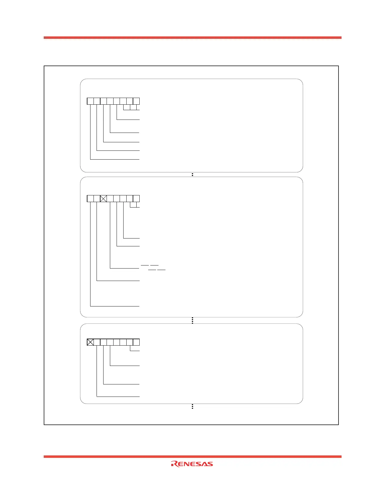
Setting UART1 transmit/receive mode register
UART1 transmit/receive mode register [Address 03A8 16]
U1MR
Invalid in clock synchronous I/O mode
Must be fixed to “001”
b7 b0
01000
Invalid in clock synchronous I/O mode
Invalid in clock synchronous I/O mode
Sleep select bit
Must be “0” in clock synchronous I/O mode
Setting UART1 transmit/receive control register 0
UART1 transmit/receive control register 0 [Address 03AC 16]
U1C0
CLK polarity select bit
0 : Transmission data is output at falling edge of transfer clock and
reception data is input at rising edge
b7 b0
100
BRG count source select bit
0 0 : f
1 is selected
0 1 : f
8 is selected
1 0 : f
32 is selected
1 1 : Inhibited
b1 b0
Valid when bit 4 = “0”
CTS/RTS disable bit
1 : CTS/RTS function disabled
Transmit register empty flag
0 : Data present in transmit register (during transmission)
1 : No data present in transmit register (transmission completed)
Transfer format select bit
0 : LSB first
Continued to the next
a
e
Setting UART transmit/receive control register 2
UART transmit/receive control register 2 [Address 03B0 16]
UCON
CLK/CLKS select bit 1
1 : Transfer clock output from multiple pins function selected
UART1 transmit interrupt cause select bit
1 : Transmission completed (TXEPT = 1)
CLK/CLKS select bit 0
0 : Clock output to CLK1
1 : Clock output to CLKS1
b7 b0
1 1
Must always be "0"
0
 Loading...


