Power Control
M30240 Group
Rev.1.00 Sep 24, 2003 Page 278 of 360
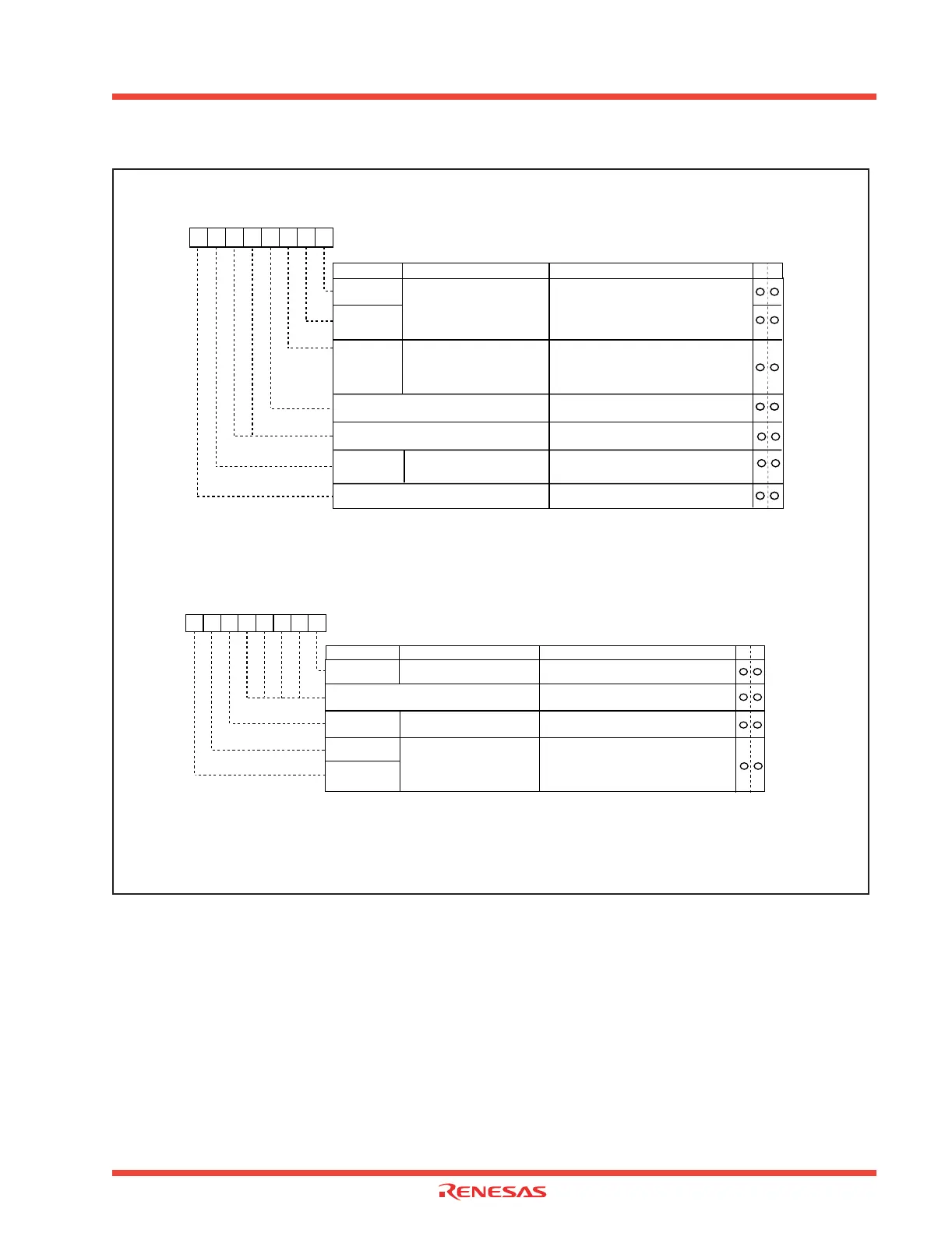
Figure 2.127: Power control related registers
System clock control register 0 (Note 1)
Note 1: Set bit 0 of the protect register (address 000A16 ) to “1” before writing
to this register.
Note 2: Changes to “1” when shifting to stop mode and at a reset.
Note 3: Peripheral clocks are f1, f8, and f32.
Symbol Address When reset
CM0 0006
16 4816
Bit name FunctionBit symbol
b7 b6 b5 b4 b3 b2 b1 b0
0 0 : I/O port P37
0 1 : Invalid
1 0 : f
8 output
1 1 : f
32 output
b1 b0
CM01
CM02
CM00
Clock output function
select bit
WAIT peripheral function
clock stop bit (Note 3)
0 : Do not stop peripheral function
clock in wait mode
1 : Stop peripheral function clock in
wait mode
WR
CM06
Main clock division select
bit 0 (Note 2)
0 : CM16 and CM17 valid
1 : Division by 8 mode
Reserved bit Always set to "1"
Reserved bit
Always set to "0"
Reserved bit
Always set to "0"
0
001
System clock control register 1 (Note 1)
Symbol
Address
When reset
CM1
0007
16
2016
Bit name FunctionBit symbol
b7 b6 b5 b4 b3 b2 b1 b0
CM10
All clock stop control bit
0 : Clock on
1 : All clocks off (stop mode)
CM15
X
IN-XOUT drive capacity
select bit (Note 2)
0 : LOW
1 : HIGH
WR
CM16
C
M17
Main clock division select
bit 1 (Note 3)
0 0 : No division mode
0 1 : Division by 2 mode
1 0 : Division by 4 mode
1 1 : Division by 16 mode
b7 b6
00
Reserved bit
Always set to
“0”
00
Note 1: Set bit 0 of the protect register (address 000A 16) to “1” before writing
to this register.
Note 2: This bit changes to “1” when shifting to stop mode and at a reset.
Note 3: Can be selected when bit 6 of the system clock control register 0
(address 0006
16
) is "0". If "1", division mode is fixed at 8.
 Loading...


