EasyManua.ls Logo

Renesas M16C Series User Manual

Renesas M16C Series
380 pages
To Next Page IconTo Next Page
To Previous Page IconTo Previous Page
Page #321 background imageLoading...
Page #321 background image
Universal Serial Bus
M30240 Group
Rev.1.00 Sep 24, 2003 Page 303 of 360
• Receive an illegal data toggle during a STATUS stage,
• Receive an illegal data toggle during a SETUP stage,
• Host requests more data than specified during the SETUP stage (receive an IN token when the
DATA_END is set),
• Host sends more data then specified during the SETUP stage (receive an OUT token when the
DATA_END is set),
• Receive larger data packet than the maximum packet (MaxP) size.
All of the conditions stated (except bad data toggle in the SETUP stage) cause the device to send a
STALL handshake for the current IN/OUT transaction. For the bad data toggle in the SETUP state, the
device sends ACK for the SETUP stage and then sends STALL for the next IN/OUT transaction. A
STALL handshake caused by the above listed conditions lasts for one transaction and terminates the
ongoing control transfer. Any packet after the STALL handshake will be seen as the beginning of a
new control transfer.
The CPU writes a “0” to clear the FORCE_STALL status bit.
• SETUP_END Flag
This becomes “1” when processing is interrupted in mid course prior to the end of the transfer of the
data size set during the control transfer and data phase processing. This bit should be cleared to “0”
by writing “1” to the SERVICED_SETUP_END bit.Once the CPU detects the SETUP_END bit as set,
it should stop accessing the FIFO to service the previous setup transaction.
If this bit should become “1” and the OUT_PKT_RDY flag simultaneously becomes “1”, that would in-
dicate that the setup processing that was established earlier has been completed and that there is a
new SETUP token inside the FIFO.
• SERVICED_OUT_PKT_RDY Bit
The OUT_PKT_RDY is cleared to “0” when this bit is set to “1”.
• SERVICED_SETUP_END Bit
The SETUP_END bit is cleared to “0” when this bit is set to “1”.
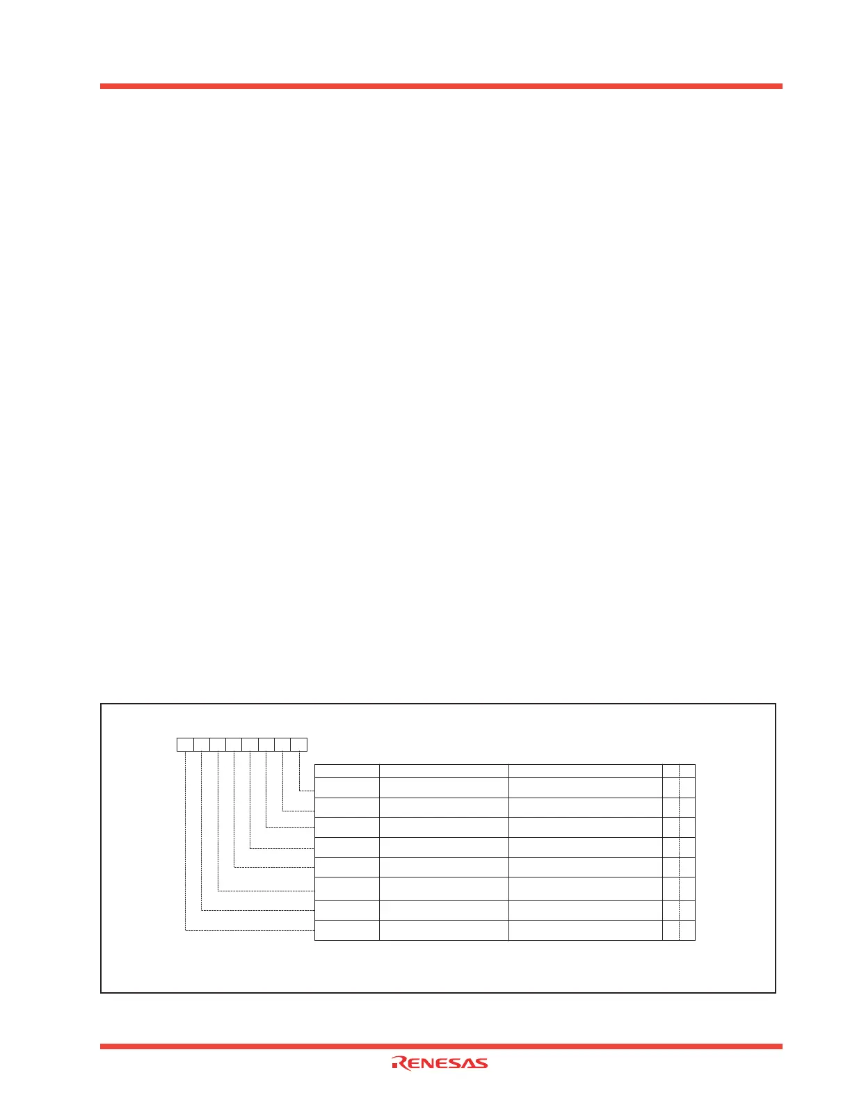
Figure 3.17 shows the structure of the USB Endpoint 0 Control/Status Register
Figure 3.17: USB Endpoint 0 Control/Status Register (EP0CS)
Bit Symbol Bit Name Function R W
EP0CSR0
OUT_PKT_RDY Flag
0: Not ready
1: Ready
O O
Symbol
EP0CS
Address
0311
16
When reset
00
16
USB Endpoint 0 Control and Status Register (Note 5)
b7 b5b6 b4 b3 b2 b1 b0
EP0CSR1
IN_PKT_RDY Bit
0: Not ready
1: Ready
O O
EP0CSR2 SEND_STALL Bit
0: No action
1: Stall Endpoint 0 by CPU
O O
Note 1
Note 2
Note 1: Read only
Note 2: Write "1" only or Read
Note 3: Write "0" only or Read
Note 4: Write only - Read "0"
Note 5: Refer to Programming Notes in Chapter 1, Section 5.5
EP0CSR3
DATA_END Bit
0: No action
1: Last packet transferred to/from FIFO
O O
EP0CSR4
FORCE_STALL Flag (Note 1)
0: No action
1: Stall Endpoint 0 by USB FCU
O O
EP0CSR5 SETUP_END Flag
0: No action
1: Control transfer ended before specific
data length transferred during data phase
O O
Note 3
Note 1
EP0CSR6
SERVICED_OUT_PKT_RDY Bit
0: No change
1: Clear OUT_PKT_RDY bit
EP0CSR7
SERVICED_SETUP_END Bit
0: No change
1: Clear SETUP_END bit
Note 4
Note 4
Note 2
O O
O O

Table of Contents

Question and Answer IconNeed help?

Do you have a question about the Renesas M16C Series and is the answer not in the manual?

Renesas M16C Series Specifications

General IconGeneral
Architecture16-bit
CoreM16C
Instruction Set ArchitectureCISC
Flash MemoryUp to 512 KB
Operating Voltage2.7V to 5.5V
Operating Temperature Range-40°C to +85°C
Package TypesLQFP, QFP
TimersMultiple 16-bit timers
ADC10-bit
Communication InterfacesUART, SPI, I2C
InterruptsMultiple interrupt sources

Summary

Chapter 1: Hardware

1.1 Description

Overview of the M30240 group as a single-chip USB peripheral microcontroller based on M16C family.

1.1.1 Features

Lists the key features of the M30240 group, including CPU, USB capabilities, memory, voltage, and peripherals.

1.1.3 Pin Configuration

Shows the pin configuration (top view) of the M30240 group, detailing each pin's name, I/O, and basic function.

1.1.4 Block Diagram

Presents a block diagram illustrating the internal structure and major components of the M30240 group.

1.1.5 Performance outline

Details the performance specifications of the M30240 group, including instruction count, memory capacity, and I/O ports.

1.1.6 Pin Description

Provides a detailed description of each pin of the M30240 microcontroller, including its name, I/O type, and functions.

CHAPTER 2: PERIPHERAL FUNCTIONS USAGE

2.1 Protect

Explains the protect function to prevent unintended changes to important registers when a program runs away.

2.2 Timer A

Provides an overview and detailed operation modes of the 16-bit Timer A, including timer, event counter, and PWM modes.

2.3 Timer B

Details the operation and registers of Timer B, a 16-bit timer that operates only in timer mode.

2.4 Clock-Synchronous Serial I/O

Explains clock-synchronous serial communication, including transmission/reception formats, transfer rates, and error detection.

2.5 Clock-Asynchronous Serial I/O (UART)

Covers UART operations, including transmission/reception formats, transfer rates, error detection, and functions like SIM interface compliance.

2.6 A-D Converter

Describes the A-D converter, its modes of operation, conversion clock, conversion time, and related registers.

2.7 DMAC

Explains the DMAC (Direct Memory Access Controller) for data transfer between memory and peripherals without CPU intervention.

2.10 Address Match Interrupt

Explains the address match interrupt functionality for simplified debugging, including enable/disable and timing.

2.11 Key-Input Interrupt

Describes the key-input interrupt, which is generated by falling edges on Port 0 or Port 1 pins used as input.

2.12 Power Control

Explains power control modes (Normal, Wait, Stop) for reducing CPU power consumption by stopping oscillators or clocks.

2.13 Programmable I/O Ports

Details the programmable I/O ports, including direction registers, port registers, pull-up control, and high drive capacity.

Chapter 3 Universal Serial Bus

3.1 Frequency Synthesizer

Explains how to set up and use the frequency synthesizer to generate the 48MHz clock for USB and DC-DC converter power.

3.2 Universal Serial Bus

Provides an overview of the Universal Serial Bus (USB) features, including specification compatibility, error handling, and transfer types.

3.2.2 USB Related Registers

Lists and describes USB-related registers for controlling USB functionality, including control, status, and enable registers.

3.2.7 USB Interrupts

Details the types of USB interrupts (Function, Reset, Resume, SOF, Suspend) and their handling via enable flags and priority levels.

3.2.8 USB Function Control Unit Initialization

Outlines the initialization routine for the USB Function Control Unit, including frequency synthesizer setup and endpoint initialization.

3.2.9 USB Control Transfers and SET_ADDRESS Request

Explains USB control transfers, the SET_ADDRESS request, and procedures for setting the device address.

Chapter 4 Interrupts

4.1 Overview of Interrupts

Provides an overview of interrupt types, including software, hardware, special, and peripheral I/O interrupts.

4.1.1 Type of Interrupts

Classifies interrupts into maskable and non-maskable types, detailing software and hardware interrupt categories.

4.1.2 Interrupt Vector Tables

Describes interrupt vector tables, including fixed and variable types, and lists interrupts assigned to fixed vector tables.

4.1.3 Interrupt Control

Explains interrupt control registers, interrupt request bits, enable flags, and priority levels for managing interrupts.

4.1.4 Interrupt Sequence

Details the sequence of operations when an interrupt occurs, including saving registers and processor control flow.

4.1.5 Multiple Interrupts

Explains how multiple interrupts are handled, including priority levels and interrupt acceptance conditions.

Chapter 5 Built-in PROM Version

5.1 Built-in PROM Version

Introduces the built-in PROM version, its functions, and available types (OTP and EPROM).

5.1.1 Outline

Outlines the capabilities of the built-in PROM version, including programming methods and suitability for different production volumes.

5.2 EPROM version

Describes the EPROM version, its operating modes (Normal, EPROM), and related pins.

5.2.1 EPROM mode pins

Lists pin functions specifically for the EPROM mode, detailing their roles in programming and verification.

5.2.2 Input/Output signals

Explains the input/output signals for Read, Program, and Erase operations in EPROM mode.

5.2.3 Algorithm Programming

Details the step-by-step algorithm for programming the built-in PROM, including voltage settings and pulse application.

5.3 Usage Precaution

Provides precautions for using built-in PROM versions, including handling of high voltage and protection of the EPROM window.

5.3.1 Built-in PROM versions

Offers specific cautions for programming built-in PROM versions, emphasizing voltage and power-on sequences.

5.3.2 One-time PROM versions

Highlights that OTP versions are not tested/screened, recommending programming and testing for reliability.

5.3.3 EPROM versions

Advises on protecting the EPROM window from light and cleaning it before erasure for optimal performance.

Chapter 6 Standard Characteristics

6.1 Standard DC Characteristics

Presents standard DC characteristics of the M30240EC, including output currents and voltage ratings.

Related product manuals