RL78/F13, F14 CHAPTER 17 LIN/UART MODULE (RLIN3)
R01UH0368EJ0210 Rev.2.10 1105
Dec 10, 2015
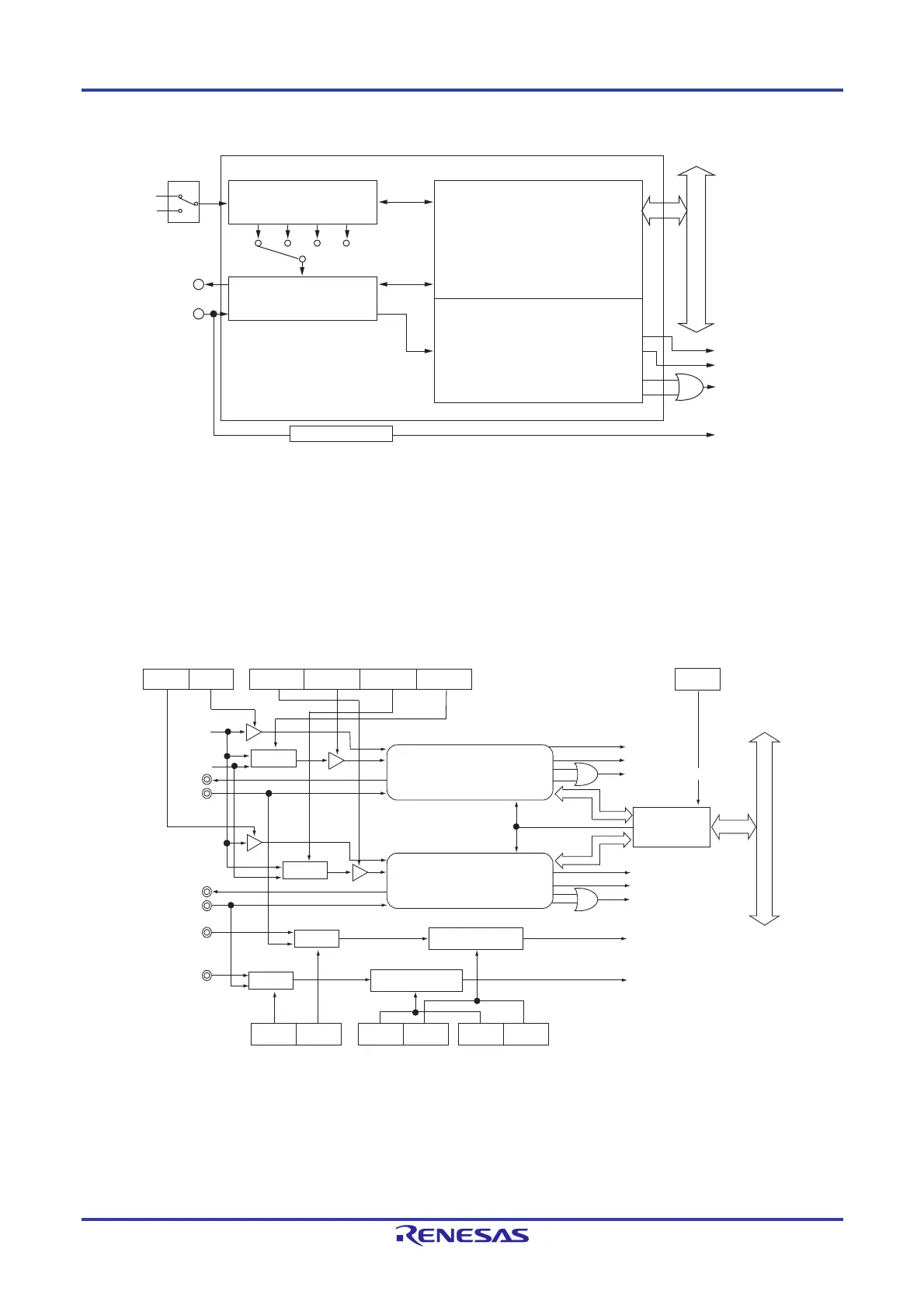
Figure 17-1. LIN/UART Module Block Diagram (1)
LTXDn, LRXDn: LIN/UART module I/O pins
LINn baud rate generator: Generates the LIN/UART module communication clock signal.
LINn registers: LIN/UART module registers
LINn interrupt controller: Controls interrupt requests generated by the LIN/UART module.
(n = 0, 1)
Figure 17-2. LIN/UART Module Block Diagram (2)
LINnMCK
fa fb fc fd
LIN/UART module
LTXDn
LRXDn
n = 0, 1
LINn registers
INTLINnTRM
INTLINnRVC
INTLINnSTA/
INTLINn
INTLINnWUP
LINn transmission interrupt
Successful LINn reception
interrupt
LINn reception status
error interrupt
LINn interrupt
LINn
interrupt control circuit
LINn baud rate generator
LINn protocol controller
f
CLK
0
1
f
MX
Edge detection circuit
Data bus
LIN1EN
PER2
LIN0EN LIN1MCKE LIN0MCKE LIN1MCK LIN0MCK
LINCKSEL LCHSEL
LSEL0
Note 4
f
CLK
f
MX
LTXD0
LRXD0
Selector
LIN/UART module channel 0
Note 4
INTLIN0TRM
INTLIN0RVC
INTLIN0STA/INTLIN0
LIN channel
select controller
Internal bus
LIN/UART module channel 1
Note 4
Edge detector
Selector
Selector
Selector
1. For details, see CHAPTER 21 INTERRUPT FUNCTIONS.
2. INTP11 is mounted only on the 80-pin products of RL78/F13 (LIN incorporated),
64- and 80-pin products of RL78/F13 (CAN and LIN incorporated), and 64-, 80-, and
100-pin products of RL78/F14.
3. INTP12 is mounted only on 64-, 80-, and 100-pin products of RL78/F14.
4. Only the registers of the channel that is selected with the LCHSEL register
can be accessed using the CPU instructions and by the DTC. For the product
incorporating one channel, set the LSEL0 bit in the LCHSEL register to 0.
ISC3 ISC2
ISC
Notes
EGP1 EGN1
EGP12 EGP11 EGN12 EGN11
Edge detector
Note 1
Note 1
INTP12/INTLIN1WUP
INTP11/INTLIN0WUP
INTP12
Note 3
INTP11
Note 2
LTXD1
LRXD1
INTLIN1TRM
INTLIN1RVC
INTLIN1STA/INTLIN1
 Loading...


