RL78/F13, F14 CHAPTER 17 LIN/UART MODULE (RLIN3)
R01UH0368EJ0210 Rev.2.10 1158
Dec 10, 2015
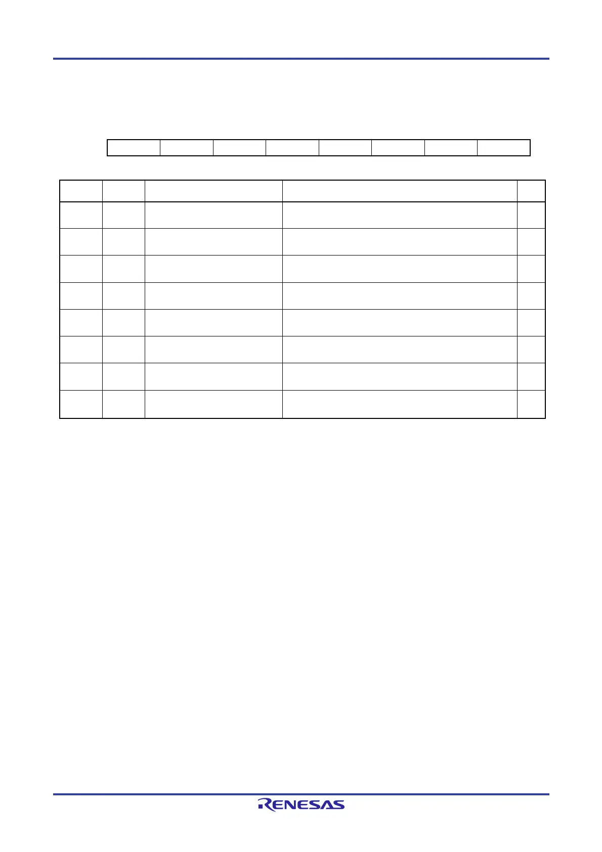
(19) LIN/UART Error Status Register (LESTn)
Address: F06D3H
7 6 5 4 3 2 1 0
RPER IPER CSER SFER FER TER — BER
Value after reset:
0 0 0 0 0 0 0 0
Bit Symbol Bit Name Function R/W
0 BER Bit Error Flag 0: Bit error has not been detected.
1: Bit error has been detected.
R/W
1 — Reserved This bit is always read as 0. The write value should always be
0.
R/W
2 TER Timeout Error Flag 0: Frame/response timeout error has not been detected.
1: Frame/response timeout error has been detected.
R/W
3 FER Framing Error Flag 0: Framing error has not been detected.
1: Framing error has been detected.
R/W
4 SFER Sync Field Error Flag 0: Sync field error has not been detected.
1: Sync field error has been detected.
R/W
5 CSER Checksum Error Flag 0: Checksum error has not been detected.
1: Checksum error has been detected.
R/W
6 IPER ID Parity Error Flag 0: ID parity error has not been detected.
1: ID parity error has been detected.
R/W
7 RPER Response Preparation Error Flag 0: Response preparation error has not been detected.
1: Response preparation error has been detected.
R/W
The LESTn register is automatically cleared to 00H upon transition to LIN reset mode.
In LIN reset mode, writing to this register is disabled. In LIN reset mode, the register retains 00H.
To clear the specific bits in the register, write 0 to the bits to be cleared and write 1 to the other bits by using an 8-bit data
transfer instruction.
BER flag (bit error flag)
Only 0 can be written to the BER flag; when 1 is written, the bit retains the value that has been retained before 1 is written.
The BER flag is set to 1 upon bit error detection if the BERE bit in the LEDEn register is 1 (bit error detection is enabled). To
clear the bit to 0, write 0 to the bit.
TER flag (timeout error flag)
Only 0 can be written to the TER flag; when 1 is written, the bit retains the value that has been retained before 1 is written.
The TER flag is set to 1 upon frame timeout error or response timeout error detection if the TERE bit in the LEDEn register
is 1 (frame/response timeout error detection is enabled). To clear the bit to 0, write 0 to the bit.
FER flag (framing error flag)
Only 0 can be written to the FER flag; when 1 is written, the bit retains the value that has been retained before 1 is written.
The FER flag is set to 1 upon framing error detection if the FERE bit in the LEDEn register is 1 (framing error detection is
enabled). To clear the bit to 0, write 0 to the bit.
SFER flag (sync field error flag)
Only 0 can be written to the SFER flag; when 1 is written, the bit retains the value that has been retained before 1 is written.
The SFER flag is set to 1 upon sync field error detection if the SFERE bit in the LEDEn register is 1 (sync field error detection
is enabled). To clear the bit to 0, write 0 to the bit.
 Loading...


