RL78/F13, F14 CHAPTER 17 LIN/UART MODULE (RLIN3)
R01UH0368EJ0210 Rev.2.10 1163
Dec 10, 2015
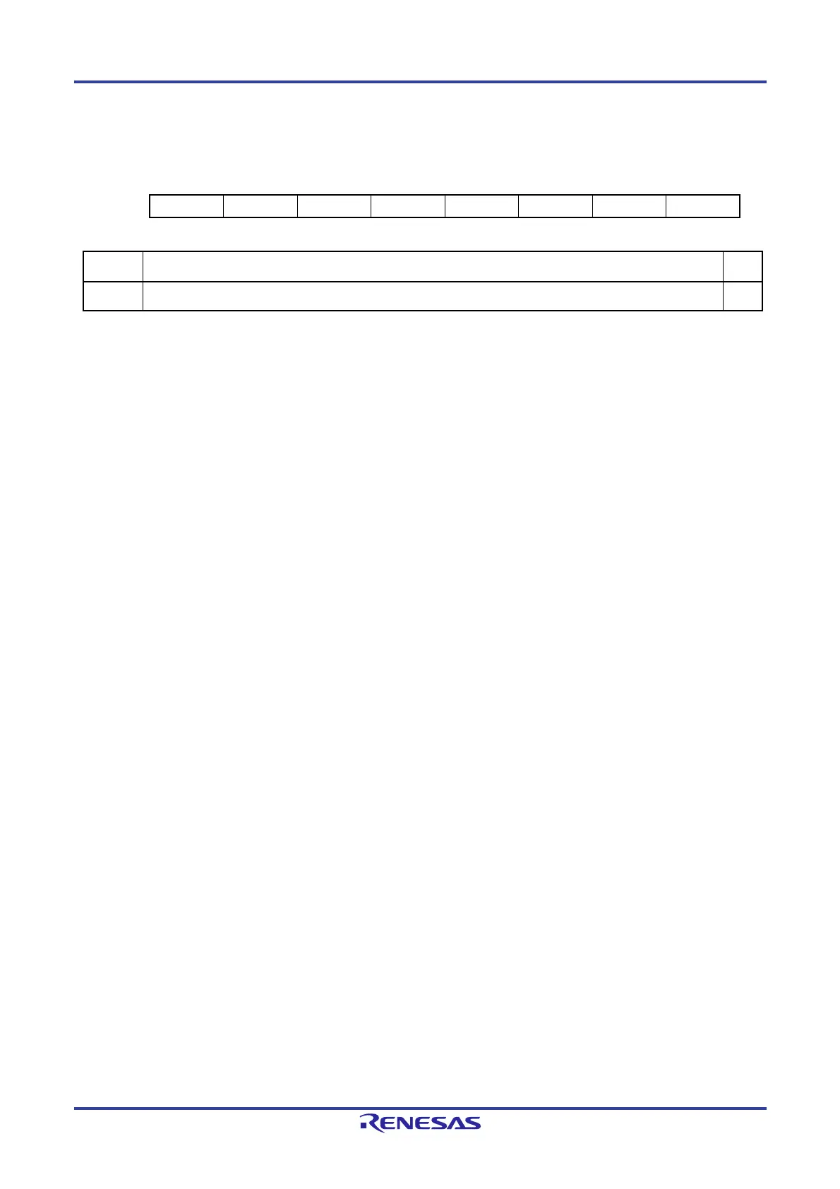
(22) LIN Checksum Buffer Register (LCBRn)
Address: F06D6H
7 6 5 4 3 2 1 0
Value after reset:
0 0 0 0 0 0 0 0
Bit Function R/W
7 to 0 Holds the checksum value transmitted or received. R/W
In LIN mode, this register operates as follows:
When the RCDS bit in the LDFCn register is 1 (transmission):
The value transmitted can be read from the register. Writing to this register is invalid.
When the RCDS bit in the LDFCn register is 0 (reception):
The value received can be read from the register. Writing to this register is invalid.
When response data of 9 bytes or more is to be transmitted or received, the checksum is appended only to the last data
group; this register is not updated for the other data groups.
In LIN self-test mode, this register operates as follows:
When the RCDS bit in the LDFCn register is 1 (transmission):
The reversed value of the value received can be read from the register after frame transmission is completed (after
loopback).
When the RCDS bit in the LDFCn register is 0 (reception):
Write the value to be received before communication. The reversed value of the value received can be read from the
register after frame transmission/reception is completed (after loopback).
For details of LIN self-test mode, refer to 17.6 LIN Self-Test Mode.
Set the LCBRn register when the FTS bit in the LTRCn register is 0 (frame transmission or wake-up transmission/reception
is halted).
 Loading...


