RL78/F13, F14 CHAPTER 25 POWER-ON-RESET CIRCUIT
R01UH0368EJ0210 Rev.2.10 1558
Dec 10, 2015
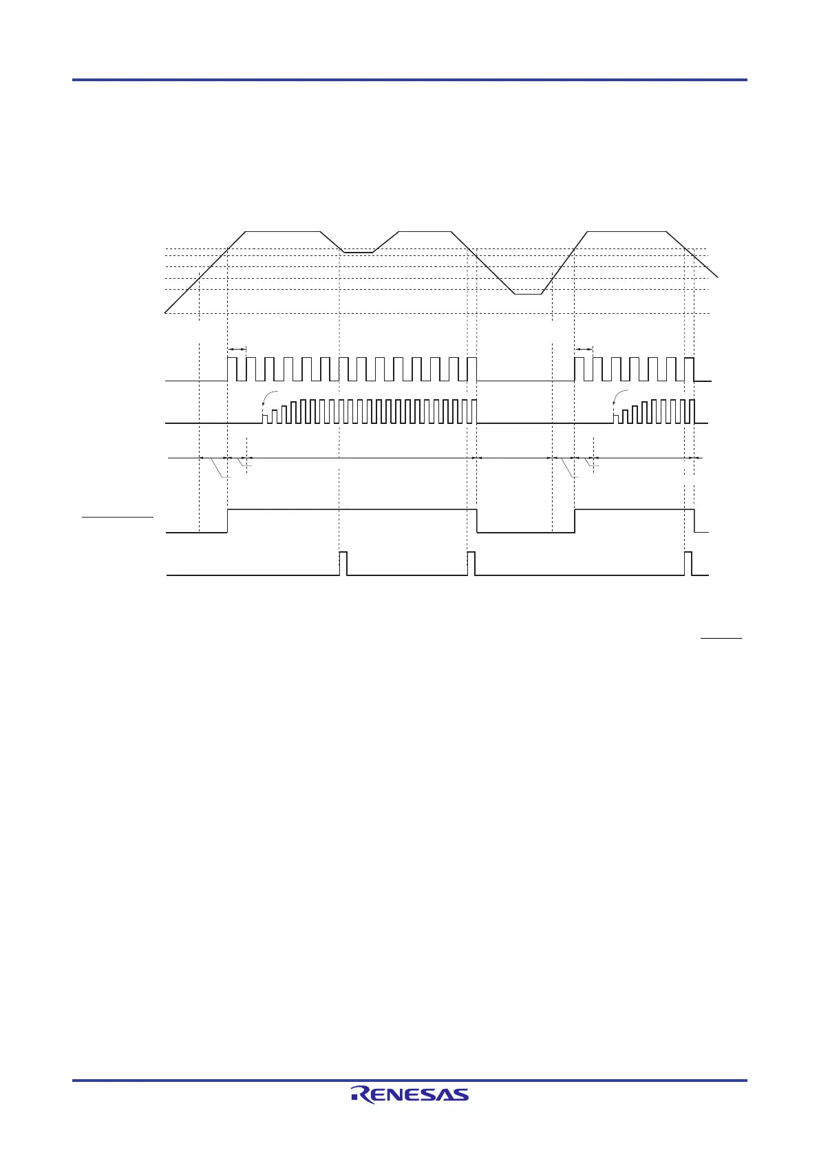
Figure 25-2. Timing of Generation of Internal Reset Signal by Power-on-reset Circuit
and Voltage Detector (2/2)
(2) When LVD is interrupt & reset mode (option byte 000C1/020C1H: LVIMDS1, LVIMDS0 = 1, 0)
Notes 1. The guaranteed range for operation is 2.7 V V
DD 5.5 V. Only proceed with normal operations after VDD
has reached or exceeded 2.7 V. If an operation may be generated at lower than 2.7V when the supply
voltage falls or power-on, use the reset function of the voltage detector, or input the low level to the RESET
pin.
2. The high-speed on-chip oscillator clock and a high-speed system clock or subsystem clock can be selected
as the CPU clock. To use the X1 clock, use the oscillation stabilization time counter status register (OSTC)
to confirm the lapse of the oscillation stabilization time. To use the XT1 clock, use the timer function for
confirmation of the lapse of the stabilization time.
3. The internal reset processing time includes the oscillation accuracy stabilization time of the high-speed on-
chip oscillator clock.
4. After the first interrupt request signal (INTLVI) is generated, the LVILV and LVIMD bits of the voltage
detection level register (LVIS) are automatically set to 1. After INTLVI is generated, appropriate settings
should be made according to Figure 26-8 Initial Setting of Interrupt and Reset Mode, taking into
consideration that the supply voltage might return to V
LVDH or higher without falling below VLVDL.
5. LVD reset processing time: 0 to 0.0701 ms (MAX.)
Remark VLVDH, VLVDL: LVD detection voltage
V
POR: POR power supply rise detection voltage
V
PDR: POR power supply fall detection voltage
0 V
Voltage stabilization wait + POR reset processing time
1.64 ms (TYP.), 3.10 ms (MAX.)
Operation
stops
Normal operation
(high-speed on-chip
oscillator clock)
Note 2
Normal operation
(high-speed on-chip
oscillator clock)
Note 2
Reset
period
(oscillation
stop)
Internal reset signal
High-speed on-chip
oscillator clock (f
IH)
High-speed
system clock (f
MX)
(when X1 oscillation
is selected)
Operation
stops
CPU
INTLVI
Note 4
Starting oscillation is
specified by software
Starting oscillation is
specified by software
Supply voltage
(V
DD
)
V
PDR
= 1.55 V (TYP.)
V
LVDH
V
POR
= 1.56 V (TYP.)
V
LVDL
Operating voltage
range lower limit
Note 1
Voltage stabilization wait + POR reset processing time
1.64 ms (TYP.), 3.10 ms (MAX.)
LVD reset processing time
Note 5
LVD reset processing time
Note 5
Wait for oscillation
accuracy stabilization
Note 3
Wait for oscillation
accuracy stabilization
Note 3
 Loading...


