Chapter 6: Maintenance and Adjustments
SPD-M20A Service Manual
49
6.3.11 Photodiode Array (PDA) Adjustment (Fine Adjustment)
NOTE
When the slit has not been adjusted in the X - X' direction the step described in 6.3.10
Slit Adjustment (Fine Adjustment), steps 1) and 2) in this section do not need to be
performed. Perform steps 3) and after.
1) Specify the 1.2 nm slit on the Optical Check software from PDA Utility.
2) Perform steps 8) through 15) described in 6.3.9 Photodiode Array (PDA) Adjustment
(Rough Adjustment) again.
3) Loosen the adjustment screw, attach a strong tape on the screw head, and fix it.
4) While the adjustment screw is loose, confirm that the half bandwidth of the emission
line is 1.18 ele max.
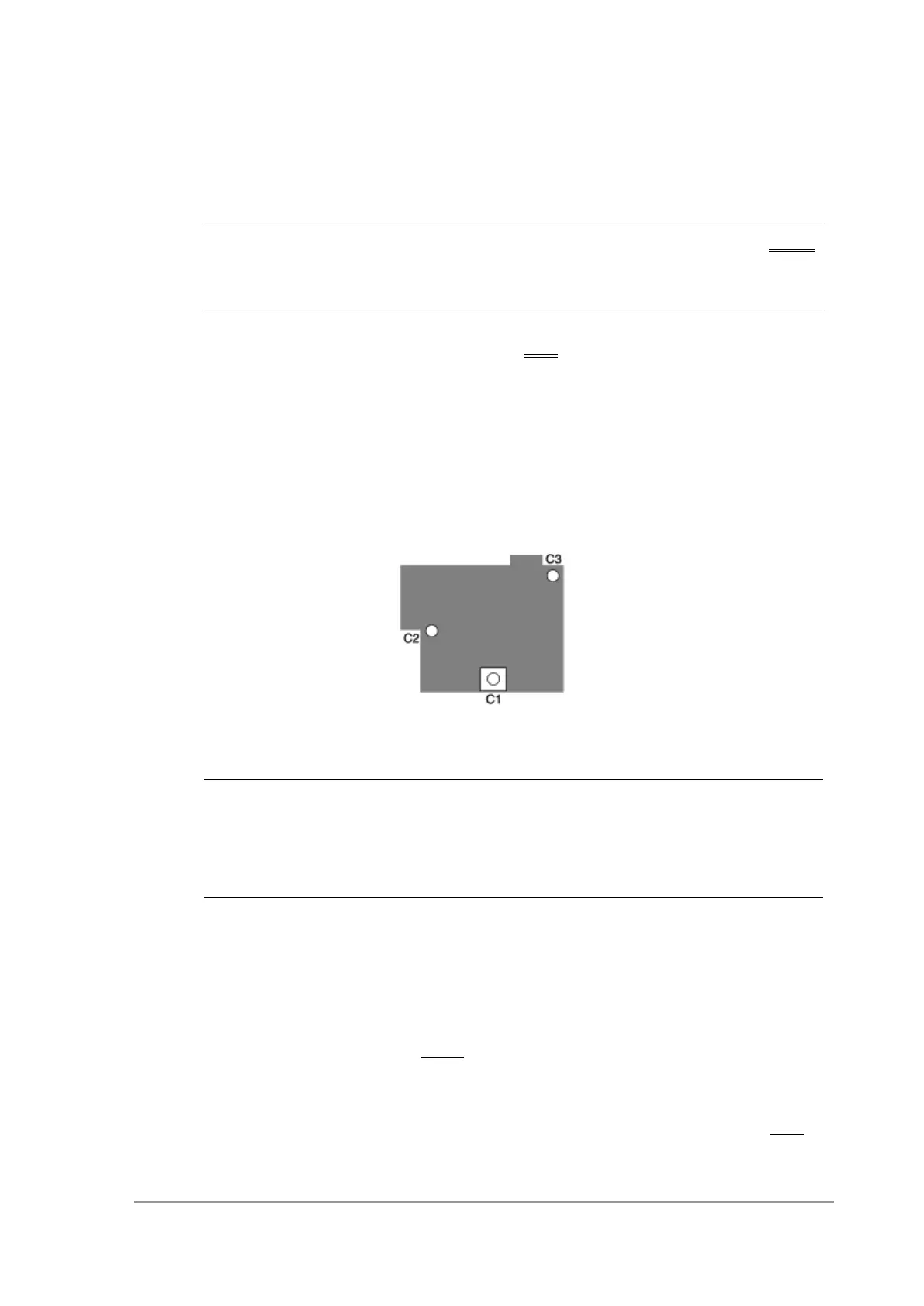
Close the cover of the optical unit and fix C1, C2, and C3 shown in the figure below in this order with
approximately 0.6 Nm of tightening torque.
Cover of the Optical Unit
NOTE
Specify the accumulation time and Y-axis displayed so that the maximum value of the
emission line does not go over 8 V.
If the lamp cover is open, an error occurs when running the software. Close the lamp
cover before starting the adjustment procedure.
6.3.12 Supplemental Information:
< If the wavelength calibration error occurs >
An error may occur during wavelength calibration at certain grating angles.
In this case, finely adjust the grating following the procedures described below.
1) Check where the peak of the Hg emission line positions between 52 ele and 72 ele by
the procedure described in 6.3.11 Photodiode Array (PDA) Adjustment (Fine
Adjustment).
2) The wavelength calibration error occurs the least when the emission line is in a range
between 60 ele and 63 ele. Adjust the position of the 0 order light described in 6.3.8
Grating Adjustment so that the emission line is in such position.
If the emission line is at 52 ele to 59 ele, move the 0 order light to the left.
 Loading...