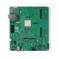
CAUTION! Do NOT plug a PC ATX power supply 6-pin connector into the ZCU216 board power connector
J50. The ATX 6-pin connector has a dierent pinout than J50. Connecng an ATX 6-pin connector into J50
damages the ZCU216 board and voids the board warranty.
See Power On/O Slide Switch for more informaon.
Zynq UltraScale+ RFSoC XCZU49DR
Configuration
Zynq UltraScale+ RFSoC ZU49DR uses a mul-stage boot process documented in the Boot and
Conguraon chapter of the Zynq UltraScale+ Device Technical Reference Manual (UG1085).
Switch SW2 conguraon opon sengs are idened in the following table.
Table 5: Mode Switch SW2 Configuration Option Settings
Mode Mode Pins [3:0] Mode SW2 [4:1]
2
JTAG 0000 ON,ON,ON,ON
QSPI32 0010
1
ON,ON,OFF,ON
SD 1110 OFF,OFF,OFF,ON
Notes:
1. Default switch setting.
2. Switch OFF = 1 = High; ON = 0 = Low. See callout 11 in Table 4.
JTAG
Vivado
®
Design Suite or third-party tools can establish a JTAG connecon to the Zynq UltraScale
+ RFSoC through the FTDI FT4232 USB-to-JTAG/USB UART device (U29) connected to micro-
USB connector (J24).
QSPI
Use the following steps to boot from the dual QSPI non-volale conguraon memory.
1. Store a valid Zynq UltraScale+ RFSoC boot image into the QSPI ash devices (U11, U12,
MIO[0:12] QSPI interface).
2. Set the boot mode pins SW2 [4:1] as indicated in the table above for QSPI32.
3. Either power-cycle or press the power-on reset (POR) pushbuon. SW2 is callout 11 in
Figure 3.
Chapter 2: Board Setup and Configuration
UG1390 (v1.1) July 10, 2020 www.xilinx.com
ZCU216 Board User Guide 20

 Loading...