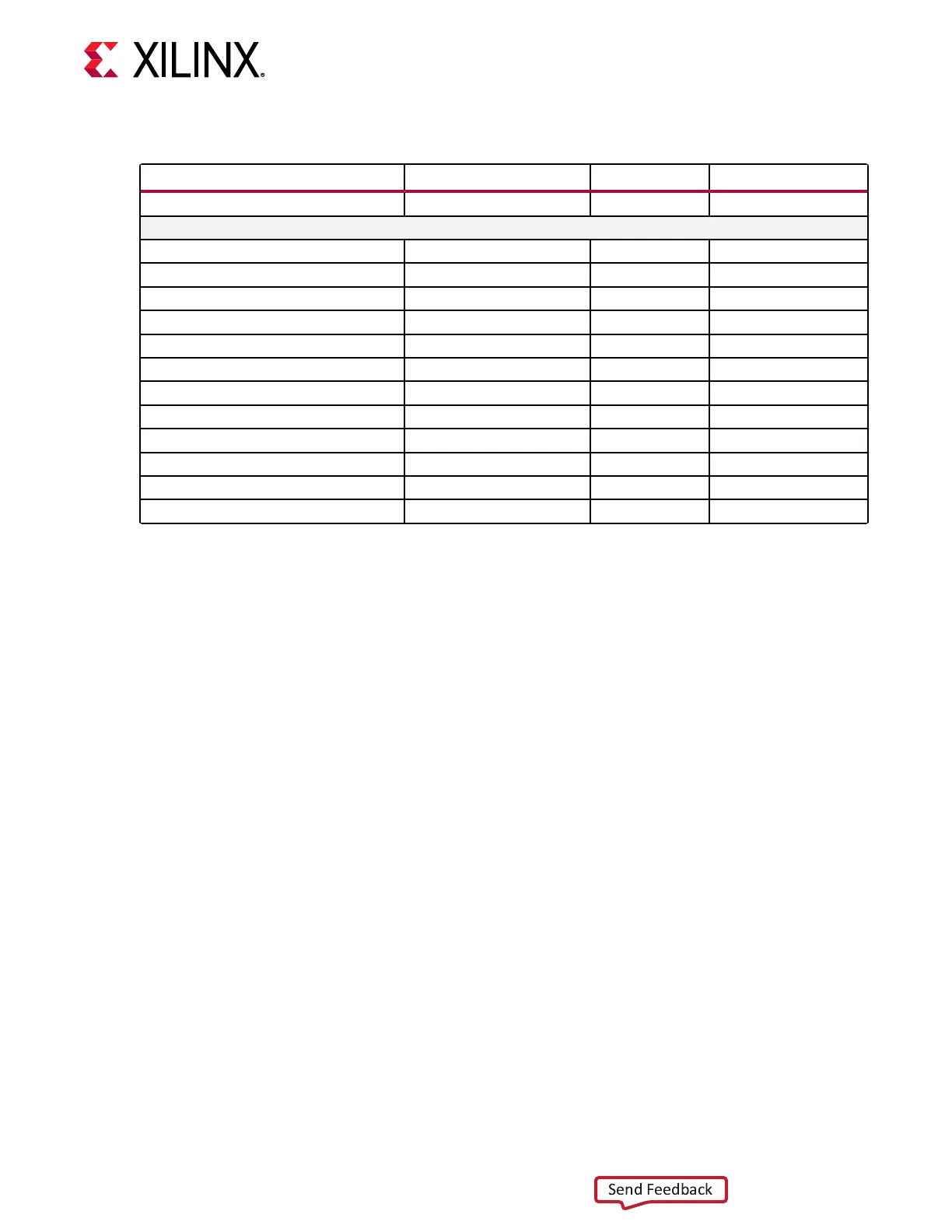
Table 18: Clock Connections to ZU49DR U1 (cont'd)
Clock Source Ref. Des. and Pin Net Name I/O Standard ZU49DR (U1) Pin
J7 USER_SMA_MGT_CLOCK_N 2 M35
U409 8A34001 eCPRI Clock
U409.A9 (Q1) 8A34001_Q1_OUT_P 2 Y39
U409.B9 (Q1) 8A34001_Q1_OUT_N 2 Y40
U409.A11 (Q2) 8A34001_Q2_OUT_P LVDS AT23
U409.B11 (Q2) 8A34001_Q2_OUT_N LVDS AT24
U409.A12 (Q3) 8A34001_Q3_OUT_P LVDS H30
U409.B12 (Q3) 8A34001_Q3_OUT_N LVDS G30
U409.M8 (Q7) 8A34001_Q7_OUT_P 2 T34
U409.L8 (Q7) 8A34001_Q7_OUT_N 2 T35
U409.A6 (Q8) 8A34001_Q8_OUT_P LVDS J21
U409.B6 (Q8) 8A34001_Q8_OUT_N LVDS H21
U409.M6 (Q11) 8A34001_Q11_OUT_P 2 Y34
U409.L6 (Q11) 8A34001_Q11_OUT_N 2 Y35
Notes:
1. U1 ZU49DR Bank 503 supports LVCMOS18 level inputs.
2. Series capacitor coupled, U1 MGT (I/O standards do not apply).
3. Series capacitor coupled.
SI5341B 10 Independent Output Any-Frequency Clock Generator U43
[Figure 2, callout 10]
• Clock generator: Silicon Labs SI5341B-D07833-GM
• Jier: <100 fs RMS typical
• Dierenal and single-ended outputs
The SI5341B data sheet addendum for the Silicon Labs SI5341B-D07833-GM documents the
pre-programmed output frequencies:
• Inputs:
○ XAXB: 48 MHz
○ Crystal Mode
○ IN0: Unused
○ IN1: Unused
○ IN2: Unused
○ FB_IN: Unused
Chapter 3: Board Component Descriptions
UG1390 (v1.1) July 10, 2020 www.xilinx.com
ZCU216 Board User Guide 46

 Loading...


