○ PL CPU reset pushbuon
○ PL User RGB LEDs (24 total, 8 each R, G, B)
○ PL PMOD0/1 (2 R.A. 2x6 Receptacles)
• Security—PSBATT buon baery backup
• SYSMON Header
• Operaonal Switches (Power on/o, PS_PROG_B, Boot mode DIP switch)
• Operaonal Status LEDs (INIT, DONE, PS STATUS, PGOOD)
• Power Management
• System Controller (MSP430)
The ZCU216 provides designers a rapid prototyping plaorm that uses the
XCZU49DR-2FFVF1760 device. The ZU49DR contains many useful processor system (PS) hard
block peripherals exposed through the mul-use I/O (MIO) interface and a variety of FPGA
programmable logic. The following table lists a brief summary of the resources available within
the ZU49DR. A feature set overview, descripon, and ordering informaon is provided in the
Zynq UltraScale+ RFSoC Data Sheet: Overview (DS889).
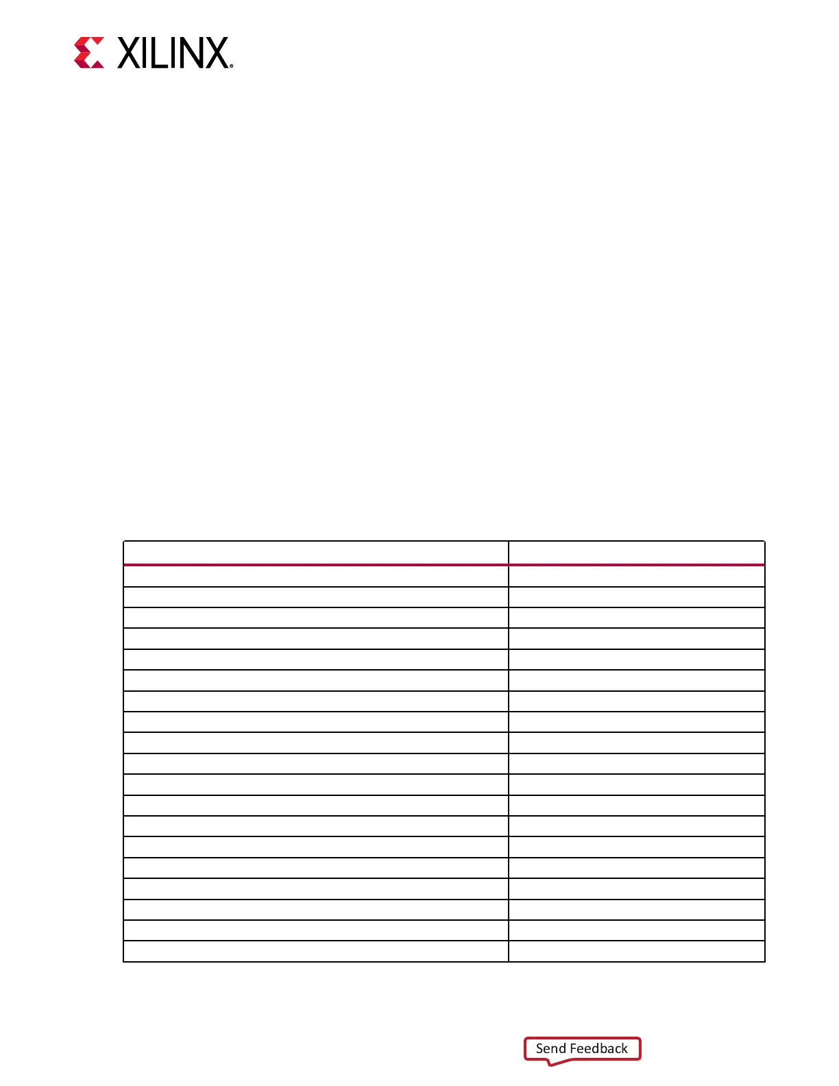
Table 1: Zynq UltraScale+ RFSoC ZU49DR Features and Resources
Feature Resource Count
14-bit 2.5 GSPS RF-DAC with DDC 16
14-bit 10 GSPS RF-DAC with DUC 16
APU: Quad-core Arm
®
Cortex™-A53 MPCore with CoreSight™ 1
RTPU: Dual-core Arm
®
Cortex™-R5F MPCore with CoreSight 1
HD I/O 96
HP I/O 312
MIO banks 3 banks, total of 78 pins
PS GTR 6 Gb/s transceivers 4 PS-GTRs
PL GTY 28 Gb/s transceivers 16 GTYs
System Logic Cells 930, 300
CLB Flip-Flops 850, 560
CLB LUTs 425, 280
Max. Distributed RAM (Mb) 13.0
Block RAM Blocks 1080 (38 Mb)
UltraRAM Blocks 80 (22.5 Mb)
DSP Slices 4,272
PCIe
®
Gen3 x16 / Gen4 x8 / CCIX (3) 2
150G Interlaken 1
100G Ethernet w/ RS-FEC 2
Chapter 1: Introduction
UG1390 (v1.1) July 10, 2020 www.xilinx.com
ZCU216 Board User Guide 9

 Loading...


