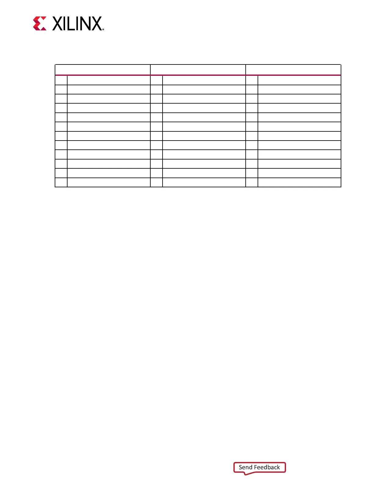
Table 7: MIO Peripheral Mapping (cont'd)
MIO[0:25] Bank 500 MIO[26:51] Bank 501 MIO[52:77] Bank 502
14 I2C0 40 SD1 66 GEM3
15 I2C0 41 SD1 67 GEM3
16 I2C1 42 SD1 68 GEM3
17 I2C1 43 Not assigned/no connect 69 GEM3
18 UART0 44 Not assigned/no connect 70 GEM3
19 UART0 45 SD1 71 GEM3
20 Not assigned/no connect 46 SD1 72 GEM3
21 Not assigned/no connect 47 SD1 73 GEM3
22 GPIO 48 SD1 74 GEM3
23 GPIO 49 SD1 75 GEM3
24 Not assigned/no connect 50 SD1 76 MDIO3
25 Not assigned/no connect 51 SD1 77 MDIO3
Quad-SPI Flash Memory (MIO 0–12)
[Figure 2, callout 5]
The Micron dual MT25QU02GCBB8E12-0SIT serial NOR ash Quad-SPI memories are capable
of holding the boot image for the Zynq UltraScale+ RFSoC. This interface is used to support
QSPI32 boot mode as dened in the Zynq UltraScale+ Device Technical Reference Manual
(UG1085).
The dual Quad-SPI ash memory located at U11/U12 provides 4 Gb of non-volale storage that
can be used for conguraon and data storage.
• Part number: MT25QU02GCBB8E12-0SIT (Micron)
• Descripon:
○ 2 Gb/256 MB
○ 2.7V – 3.6V 24-ball TBGA
○ 90 MHz DTR/133 MHz STR
• Datapath width: 8 bits
• Data rate: Various depending on Single/Dual/Quad mode
The conguraon and Quad-SPI secon of the Zynq UltraScale+ Device Technical Reference Manual
(UG1085) provides details on using the Quad-SPI ash memory. For more QSPI details, see the
Micron MT25QU02GCBB8E12-0SIT data sheet on the Micron Technology website.
The detailed RFSoC connecons for the feature described in this secon are documented in the
ZCU216 board XDC le, referenced in Appendix B: Xilinx Design Constraints.
Chapter 3: Board Component Descriptions
UG1390 (v1.1) July 10, 2020 www.xilinx.com
ZCU216 Board User Guide 29

 Loading...


