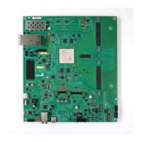
The Zynq UltraScale+ RFSoC PS block has two major processing units:
• Cortex-A53 applicaon processing unit (APU)-ARM v8 architecture-based 64-bit quad-core
mulprocessing CPU.
• Cortex-R5F real-me processing unit (RPU)-ARM v7 architecture-based 32-bit dual real-me
processing unit with dedicated ghtly coupled memory (TCM).
The Zynq UltraScale+ RFSoC PS has four high-speed serial I/O (HSSIO) interfaces supporng the
following protocols:
• Integrated block for PCI Express
®
interface-PCIe
®
base specicaon version 2.1 compliant.
• SATA 3.1 specicaon compliant interface.
• USB 3.0 interface-compliant to USB 3.0 specicaon implemenng a 5 Gb/s line rate.
• Serial GMII interface-supports a 1 Gb/s SGMII interface.
The PS and PL can be coupled with mulple interfaces and other signals to eecvely integrate
user-created hardware accelerators and other funcons in the PL logic that are accessible to the
processors. They can also access memory resources in the processing system. The PS I/O
peripherals, including the stac/ash memory interfaces share a mulplexed I/O (MIO) of up to
78 MIO pins. Zynq UltraScale+ RFSoCs can also use the I/O in the PL domain for many of the PS
I/O peripherals. This is done through an extended mulplexed I/O interface (EMIO) and boots at
power-up or reset.
For addional informaon on Zynq UltraScale+ RFSoC, see the Zynq UltraScale+ RFSoC Data
Sheet: Overview (DS889) and the Zynq UltraScale+ Device Technical Reference Manual (UG1085) for
more informaon about conguraon opons for the Zynq UltraScale+ RFSoC.
Encryption Key Battery Backup Circuit
The Zynq UltraScale+ RFSoC ZU49DR U1 implements bit stream encrypon key technology. The
ZCU216 board provides the encrypon key backup baery circuit shown in the gure below.
Chapter 3: Board Component Descriptions
UG1390 (v1.1) July 10, 2020 www.xilinx.com
ZCU216 Board User Guide 24

 Loading...