• Descripon:
○ 8 Gb (1 Gb x 8)
○ 1.2V 78-ball FBGA
○ DDR4-2666
The ZCU216 ZU49DR RFSoC PL DDR interface performance is documented in the Zynq
UltraScale+ RFSoC Data Sheet: DC and AC Switching Characteriscs (DS926).
The ZCU216 board DDR4 32-bit component memory interface adheres to the constraints
guidelines documented in the PCB guidelines for DDR4 secon of UltraScale Architecture PCB
Design User Guide (UG583). The ZCU216 DDR4 component interface is a 40Ω impedance
implementaon. Other memory interface details are also available in the UltraScale Architecture-
Based FPGAs Memory IP LogiCORE IP Product Guide (PG150).
For addional details, see the Micron MT40A1GWE-075E data sheet on the Micron Technology
website.
The detailed RFSoC connecons for the feature described in this secon are documented in the
ZCU216 board XDC le, referenced in Appendix B: Xilinx Design Constraints.
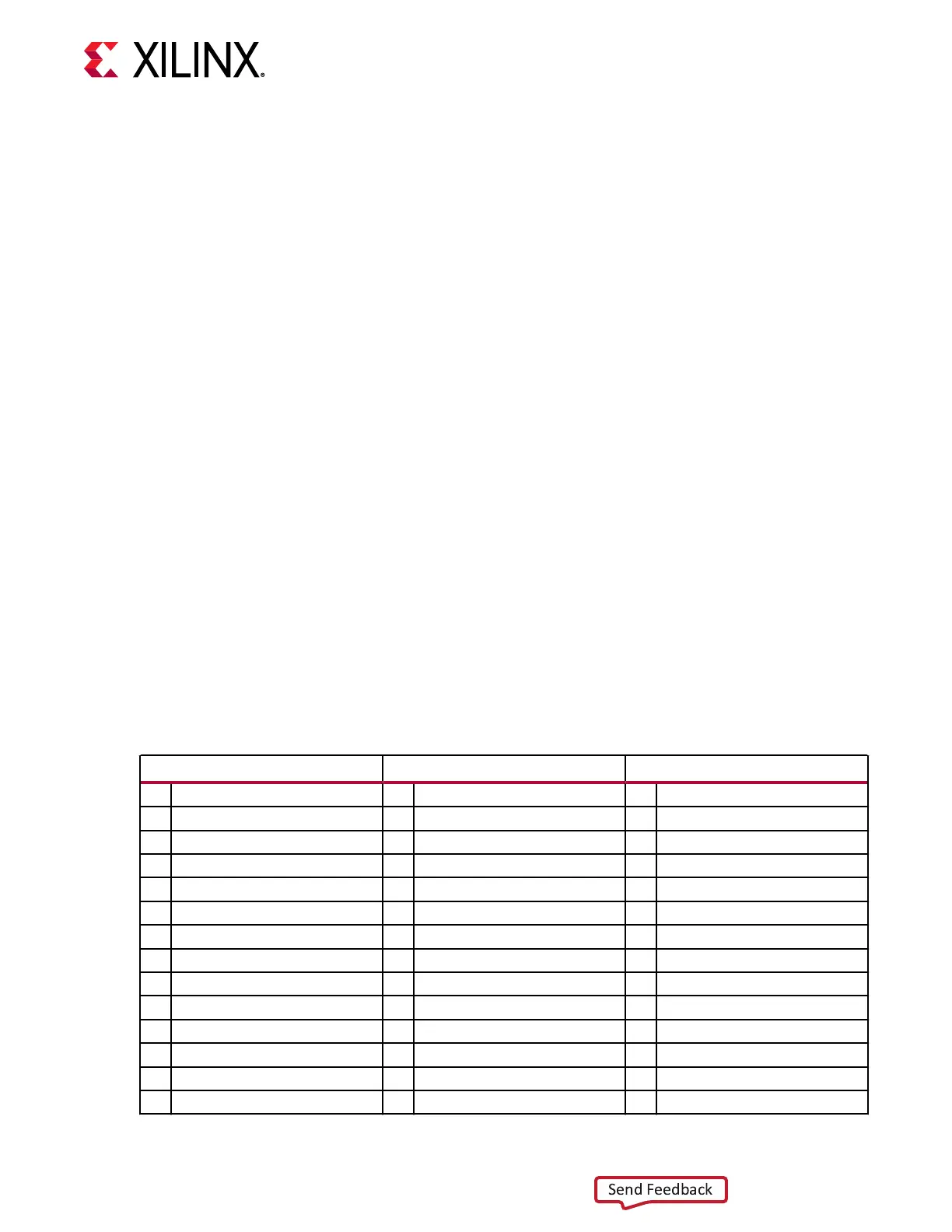
PSMIO
The following table provides PS MIO peripheral mapping implemented on the ZCU216 board.
See the Zynq UltraScale+ Device Technical Reference Manual (UG1085) for more informaon on PS
MIO peripheral mapping.
Table 7: MIO Peripheral Mapping
MIO[0:25] Bank 500 MIO[26:51] Bank 501 MIO[52:77] Bank 502
0 QSPI_LWR 26 PMU IN 52 USB0
1 QSPI_LWR 27 Not assigned/no connect 53 USB0
2 QSPI_LWR 28 Not assigned/no connect 54 USB0
3 QSPI_LWR 29 Not assigned/no connect 55 USB0
4 QSPI_LWR 30 Not assigned/no connect 56 USB0
5 QSPI_LWR 31 Not assigned/no connect 57 USB0
6 Not assigned/no connect 32 PMU GPO 58 USB0
7 QSPI_UPR 33 PMU GPO 59 USB0
8 QSPI_UPR 34 PMU GPO 60 USB0
9 QSPI_UPR 35 PMU GPO 61 USB0
10 QSPI_UPR 36 PMU GPO 62 USB0
11 QSPI_UPR 37 PMU GPO 63 USB0
12 QSPI_UPR 38 GPIO 64 GEM3
13 GPIO 39 SD1 65 GEM3
Chapter 3: Board Component Descriptions
UG1390 (v1.1) July 10, 2020 www.xilinx.com
ZCU216 Board User Guide 28

 Loading...


