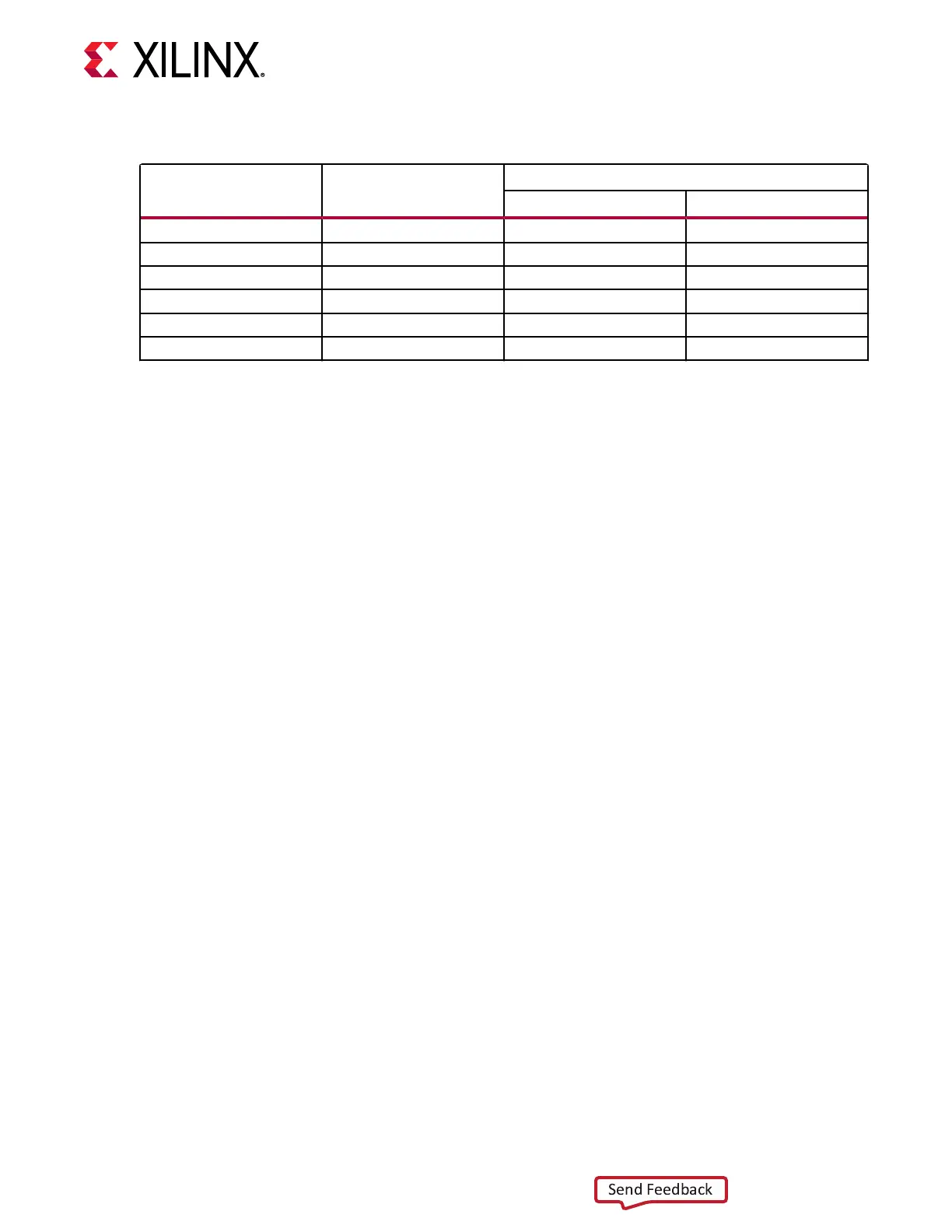
Table 14: XCZU49DR to MSP430 Connections
XCZU49DR (U1) Pin Net Name
MSP430 U38
Pin Name Pin Number
E32 MIO37_PMU_GPO5 P1_0 13
E31 MIO36_PMU_GPO4 P1_1 14
C33 MIO35_PMU_GPO3 P1_2 15
D31 MIO34_PMU_GPO2 P1_3 16
D32 MIO33_PMU_GPO1 P1_4 17
D34 MIO32_PMU_GPO0 P1_5 18
Through the I2C0 bus U1 PS-side MIO[14:15] pins, the PMU has access to the board power
controller PMBus bus (IRPS5401_SDA/SCL) and power monitor PMBus (INA226_PMBUS_SDA/
SCL). See Figure 7 for addional details.
Refer the Zynq UltraScale+ Device Technical Reference Manual (UG1085) for details about the PMU
interface.
The detailed RFSoC connecons for the feature described in this secon are documented in the
ZCU216 board XDC le, referenced in Appendix B: Xilinx Design Constraints.
SDIO (MIO 39-51)
A PS-side interface to an SD card connector is provided for boong and le system storage. This
interface is used for the SD boot mode and supports SD3.0 access post boot.
SD Card Interface
[Figure 2, callout 7]
The ZCU216 board includes a secure digital input/output (SDIO) interface to provide access to
general purpose non-volale SDIO memory cards and peripherals. Informaon for the SD I/O
card specicaon can be found on the SanDisk Corporaon or SD Associaon websites. The
ZCU216 SD card interface supports the SD1_LS conguraon boot mode documented in the
Zynq UltraScale+ Device Technical Reference Manual (UG1085).
The SDIO signals are connected to ZU49DR RFSoC PS bank 501 which has its VCCMIO set to
1.8V. The six SD interface nets MIO[46:49]_SDIO_DAT[0:3], MIO50_SDIO_CMD, and
MIO51_SDIO_CLK each have a series 30Ω resistor at the Bank 501 source. An NXP
IP4856CX25 SD 3.0-compliant voltage level-translator U23 is present between the ZU49DR
RFSoC and the SD card connector (J23). The NXP IP4856CX25 U23 device provides SD3.0
capability with SDR104 performance.
The following gure shows the connecons of the SD card interface on the ZCU216 board.
Chapter 3: Board Component Descriptions
UG1390 (v1.1) July 10, 2020 www.xilinx.com
ZCU216 Board User Guide 37

 Loading...


