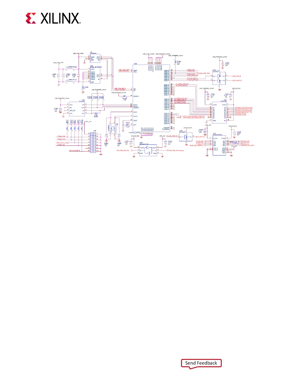
Figure 9: ZCU216 FT4232HL Connectivity
For more informaon on the FT4232HL, see the Future Technology Devices Internaonal Ltd.
website.
The detailed RFSoC connecons for the feature described in this secon are documented in the
ZCU216 board XDC le, referenced in Appendix B: Xilinx Design Constraints.
GPIO (MIO 22-23)
PS-side pushbuon SW1 is connected to MIO22 (pin U1.AL27). PS-side LED DS1, physically
placed adjacent to the pushbuon, is connected to MIO23 (pin U1.AM27).
PMU GPI (MIO 26)
PS-side MIO 26 is reserved as an input to the PMU for indicang a warm boot. PS bank 501
MIO26 (U1.A34) is connected to the I2C0 U15 TCA6416A bus expander (port P02 U15.6)
through level-shier U27. Refer to the Zynq UltraScale+ Device Technical Reference Manual
(UG1085) for details about the PMU interface.
PMU GPO (MIO 32-37)
The plaorm management unit (PMU) within the Zynq UltraScale+ RFSoC signals power domain
changes using the PMU output pins for deep-sleep mode. The Zynq UltraScale+ RFSoC PMU
GPO pins are connected to inputs of the MSP430 system controller through the TXS0108E level-
shier U37. The RFSoC U1 Bank 501 and MSP430 U38 pin numbers are listed in the following
table.
Chapter 3: Board Component Descriptions
UG1390 (v1.1) July 10, 2020 www.xilinx.com
ZCU216 Board User Guide 36

 Loading...


