EasyManuals Logo

Avnet Qseven MSC Q7-BT User Manual

Avnet Qseven MSC Q7-BT
113 pages
To Next Page IconTo Next Page
To Previous Page IconTo Previous Page
Page #38 background imageLoading...
Page #38 background image
MSC Q7-BT MSC_Q7-BT_User_Manual.pdf 38 / 113
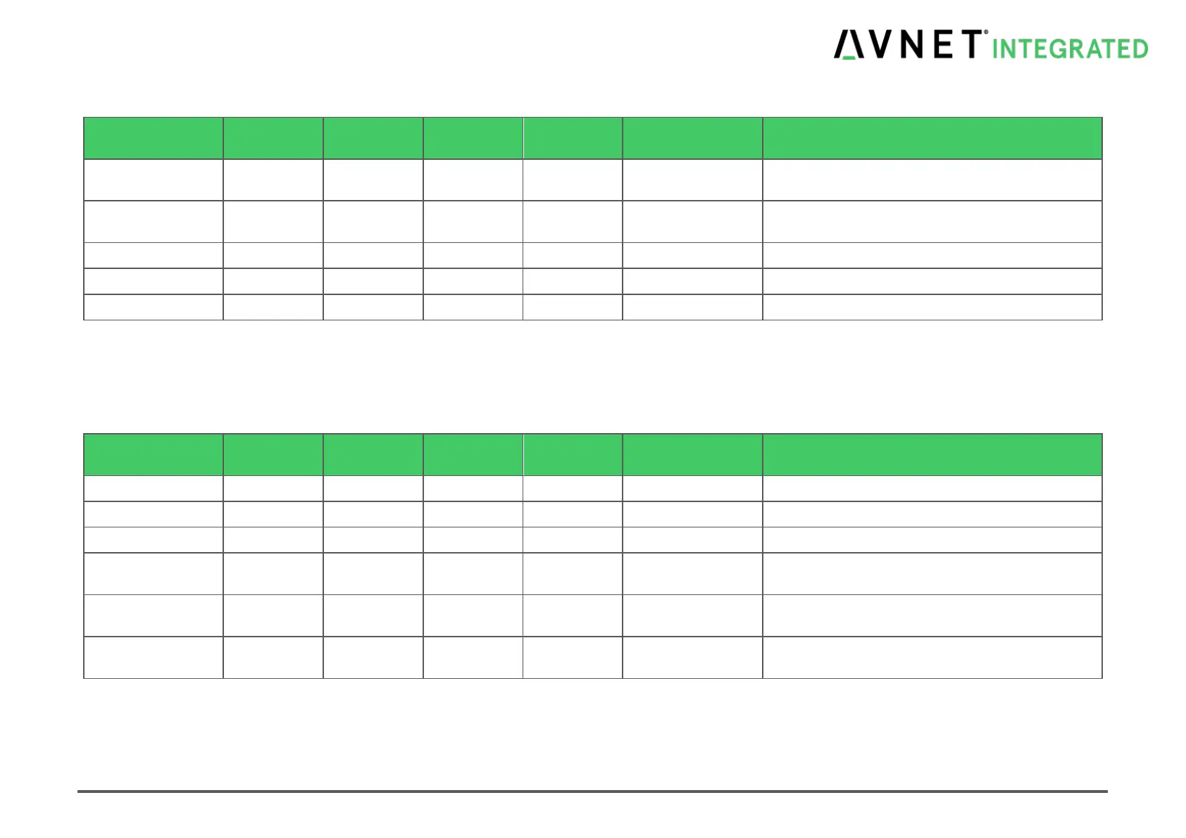
Table 4-10 HDMI Signal Description
Signal
Pin Type
Signal Level
Available
Power
Tolerance
PU/PD
Description
TMDS_LANE[0..3]+
TMDS_LANE[0..3]-
O
DP
Full On
AC coupled
on module
TMDS differential signal pair [0:3]
TMDS_CLK+
TMDS_CLK-
O
DP
Full On
AC coupled
on module
CLK+ PD 100k
CLK- PU 100k 3.3V
TMDS differential clock
HDMI_HPD#
I
3.3V CMOS
Full On
3.3V
PU 10k 3.3V
HDMI Hot Plug Detect
HDMI_CTRL_CLK
O OD
3.3V CMOS
Full On
3.3V
PU 10k 3.3V
HDMI DDC clock line
HDMI_CTRL_DAT
I/O OD
3.3V CMOS
Full On
3.3V
PU 10k 3.3V
HDMI DDC data line
4.9 SPI Bus
Table 4-11 SPI Signal Description
Signal
Pin Type
Signal Level
Available
Power
Tolerance
PU/PD
Description
SPI_MOSI
O PP
3.3V CMOS
Full On
3.3V
Master Output Slave Input
SPI_MISO
I
3.3V CMOS
Full On
3.3V
Master Input Slave Output
SPI_SCK
O PP
3.3V CMOS
Full On
3.3V
Clock
SPI_CS0#
O PP
3.3V CMOS
Full On
3.3V
When asserted low, the off-module BIOS flash
device is selected
SPI_CS1#
O PP
3.3V CMOS
Full On
3.3V
When asserted low, a SPI peripheral device is
selected
BIOS_DISABLE#
I
3.3V CMOS
Suspend
3.3V
PU 10k 3.3V SUS
Module BIOS disable input.
Pull low to disable module BIOS.

Table of Contents

Questions and Answers:

Question and Answer IconNeed help?

Do you have a question about the Avnet Qseven MSC Q7-BT and is the answer not in the manual?

Avnet Qseven MSC Q7-BT Specifications

General IconGeneral
BrandAvnet
ModelQseven MSC Q7-BT
CategoryControl Unit
LanguageEnglish

Related product manuals