Physical Interface AW00089317000
68 Basler ace GigE
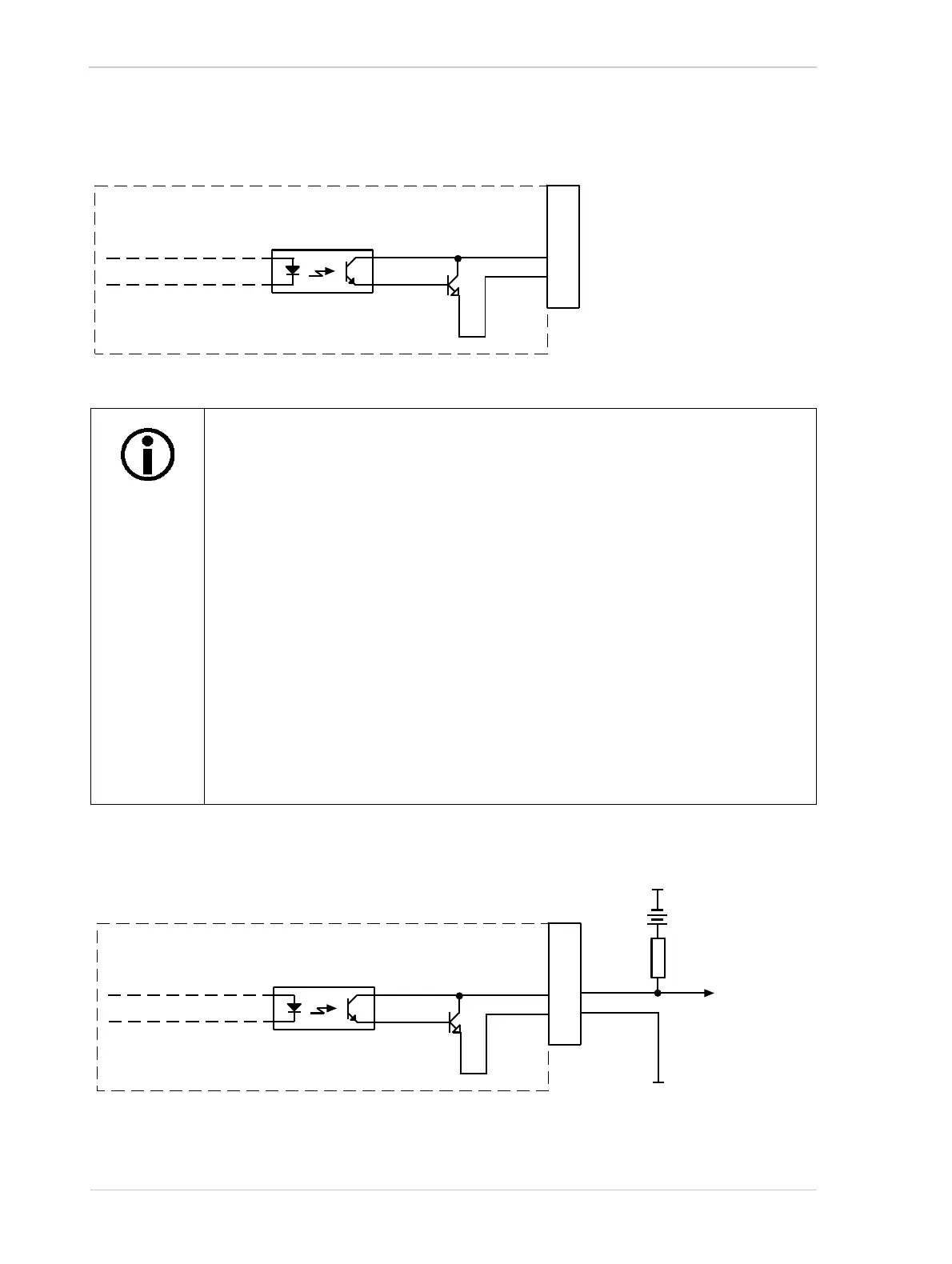
A high output signal from the camera results in a conducting Q1 transistor in the output circuit.
Figure 43 shows a typical circuit you can use to monitor the output line with a voltage signal.
On early production cameras with firmware versions of V0.x-x, the logic for the
output circuit was different. On these cameras:
A low output signal from the camera on Out_1_Ctrl results in a conducting Q1
transistor.
A high output signal from the camera results in a non-conducting Q1
transistor.
If you are using both older and newer cameras in your application, the difference
in the behavior of the output may be a problem. One way that you can address the
situation is to apply the invert function to the output on the older cameras. This will
make the behavior of the output on the older cameras match the behavior on the
newer cameras.
You could also choose to apply the invert function to the output on the newer
cameras, and this would make the behavior of the newer cameras match the
behavior of the older ones.
For more information about the invert function on the output, see Section 6.2.3 on
page 76.
1
2
3
4
5
6
6-Pin
Receptacle
I/O_Out_1
I/O_Gnd
Q1
Camera
Fig. 42: Output Line Schematic (Simplified)
Fig. 43: Typical Voltage Output Circuit (Simplified Example)
Your
Gnd
Your
Gnd
+3.3 to +24
VDC
1
2
3
4
5
6
6-Pin
Receptacle
I/O_Out_1
I/O_Gnd
Out_1_Ctrl
Camera
Voltage
Output
Signal
to You
Q1
 Loading...