CURTISS-WRIGHT 1
826448 VERSION 5 MARCH 2015 PROPRIETARY A-43
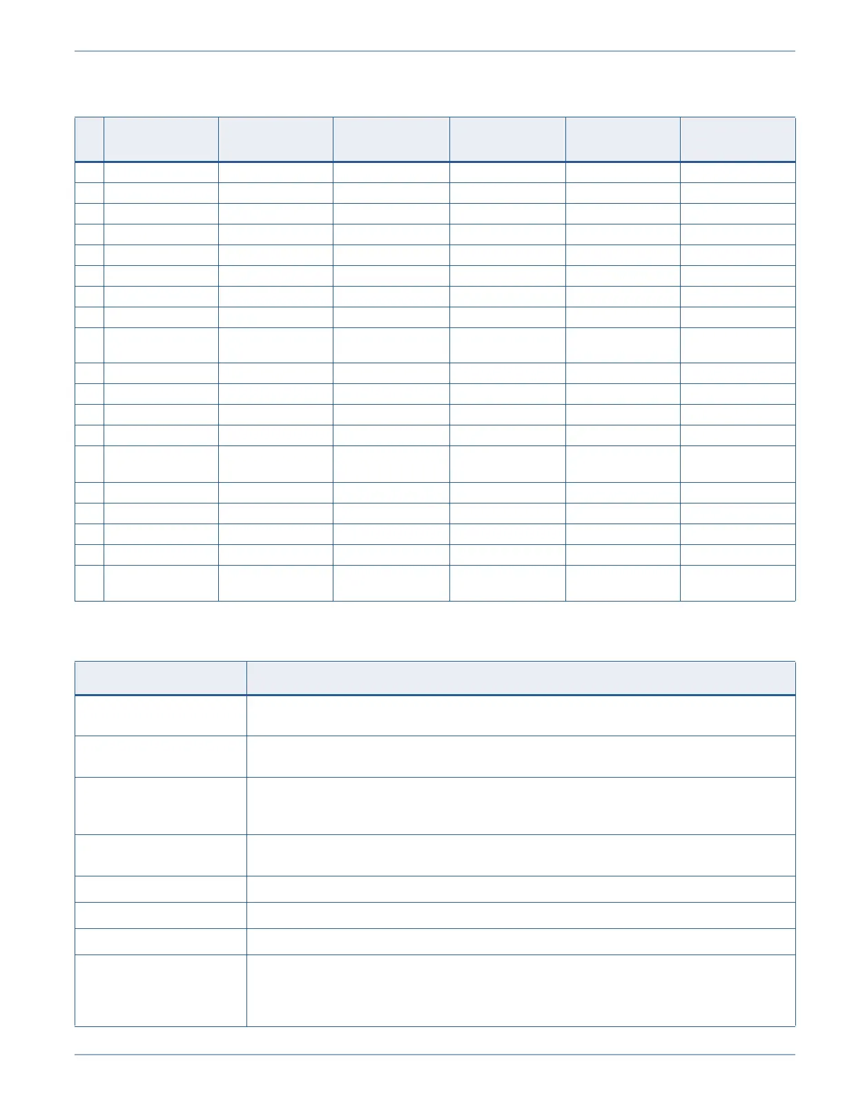
Table A.26: J15 Primary XMC Connector Pin Assignments
Pin
No.
Row A
Signal
Row B
Signal
Row C
Signal
Row D
Signal
Row E
Signal
Row F
Signal
1 XMC_TX_P0 XMC_TX_N0 3V3 XMC_TX_P1 XMC_TX_N1 12V0
2 GND GND XMC_TRST_L GND GND XMC_RST_L
3 XMC_TX_P2 XMC_TX_N2 3V3 XMC_TX_P3 XMC_TX_N3 12V0
4 GND GND XMC_TCK GND GND XMC_RSTIN_L
5 XMC_TX_P4 XMC_TX_N4 3V3 XMC_TX_P5 XMC_TX_N5 12V0
6 GND GND XMC_TMS GND GND P12V
7 XMC_TX_P6 XMC_TX_N6 3V3 XMC_TX_P7 XMC_TX_N7 12V0
8 GND GND XMC_TDI GND GND N12V
9BGA_XMC_
GPIO_0
BGA_XMC_
GPIO_1
AT_BTEI_L BGA_XMC_
GPIO_2
BGA_XMC_
GPIO_3
12V0
10 GND GND XMC_TDO GND GND XMC_GA0
11 XMC_RXZ_P0 XMC_RXZ_N0 XMC_MBIST_L XMC_RXZ_P1 XMC_RXZ_N1 12V0
12 GND GND XMC_GA1 GND GND XMC_PRESENT_L
13 XMC_RXZ_P2 XMC_RXZ_N2 3V3_AUX XMC_RXZ_P3 XMC_RXZ_N3 12V0
14 GND GND XMC_GA2 GND GND SMB_THERM_
DATA
15 XMC_RXZ_P4 XMC_RXZ_N4 AT_VCCO XMC_RXZ_P5 XMC_RXZ_N5 12V0
16 GND GND XMC_F_NVMRO GND GND SMB_THERM_CLK
17 XMC_RXZ_P6 XMC_RXZ_N6 RFU_J25_C17 XMC_RXZ_P7 XMC_RXZ_N7 RFU _F17
18 GND GND AT_MTEI_L/RFU GND GND AT_SCL/ RFU
19 B_CLK_PCH_
SRC0_P
B_CLK_PCH_
SRC0_N
AT_LBAT_L/RFU XMC_WAKE_L XMC_ROOT_L AT_SDA/RFU
Table A.27: J15 Primary XMC Connector Signal Definitions
XMC Signal Description
XMC_TX/RXZ_P/N[0:7] Differential Transmit/Receive. These signals are used by the XMC to transmit / receive high-speed
protocol-specific data to the carrier over the PCI Express interface.
B_CLK_PCH_SRC0_P/N Differential reference clock for the PCI Express interface link. This signal is generated by the carrier
and transmitted to the mezzanine.
XMC_WAKE_L An open-drain, active low signal that is driven low by an XMC PCI Express function to reactivate
the links main power rails and reference clocks. The CHAMP-AV8 does not support XMC wake
functionality and pulls the signal up to 3.3V AUX.
XMC_ROOT_L This signal shall be driven low by the carrier to enable the Root Complex features of a Processor
XMC. The CHAMP-AV8 does not support this feature and pulls the signal up to 3.3V.
SMB_THERM_CLK I2C serial clock.
SMB_THERM_DATA I2C serial data
XMC_GA0:2 I2C channel select. These are inputs to the XMC and are driven as 011 on the CHAMP-AV8.
XMC_MBIST_L XMC Built In Self Test. This signal is an output from the XMC and allows the carrier to determine
whether an XMC has completed its built-in self test. If this signal is used by the XMC, it shall be
asserted low at the de-assertion of MRSTI_L to indicate that the XMC is performing self-test and is
not yet ready.
Artisan Technology Group - Quality Instrumentation ... Guaranteed | (888) 88-SOURCE | www.artisantg.com