CURTISS-WRIGHT PRODUCT OVERVIEW
826448 VERSION 5 MARCH 2015 PROPRIETARY 1-35
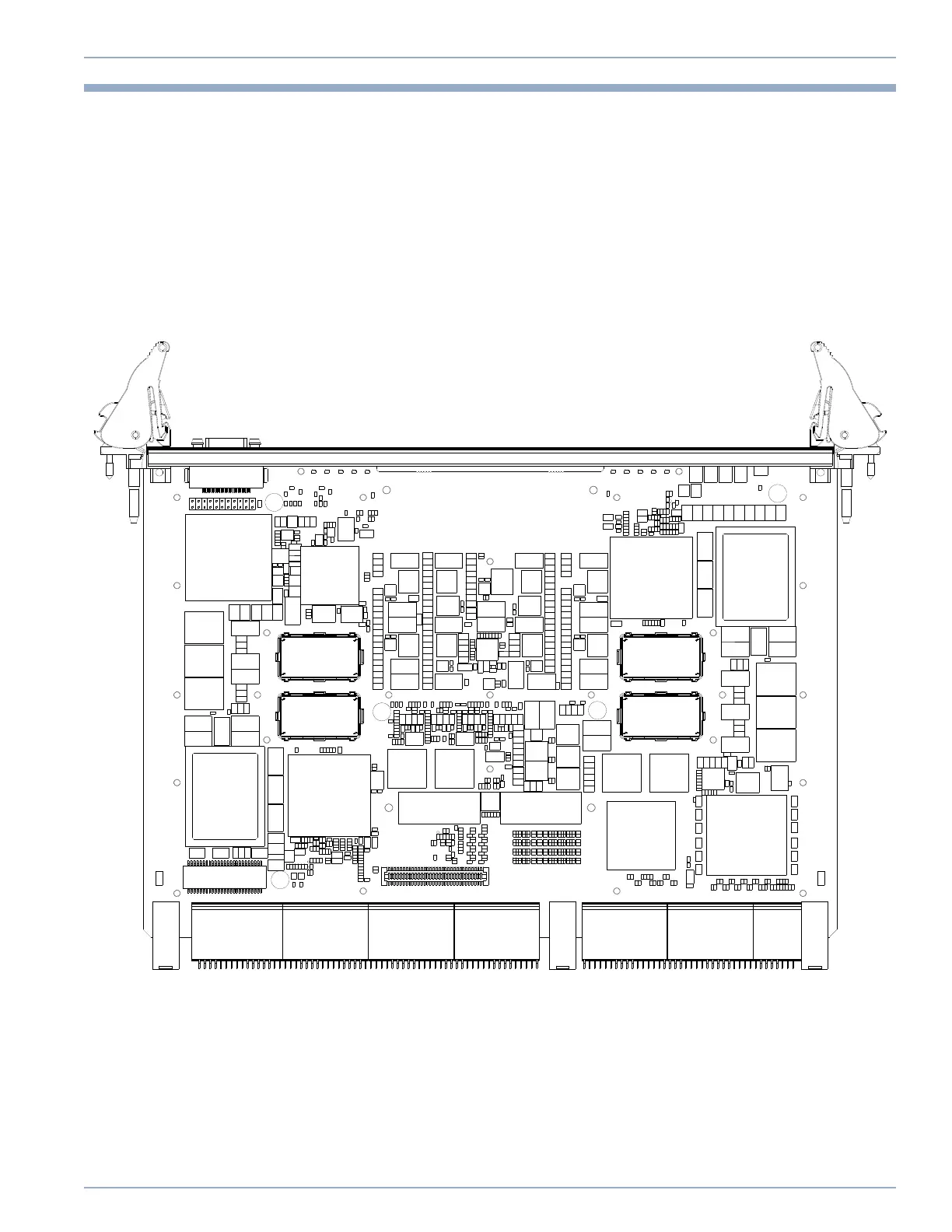
PHYSICAL CHARACTERISTICS
Figure 1.15 shows the location of the major components and the mating connectors on the
top side of the CHAMP-AV8 (some hardware has been removed from this drawing to make all
of the components visible).
All ruggedization levels of the CHAMP-AV8 board have a thermal shunt that covers some of
the components.
Figure 1.15: CHAMP-AV8 Board Layout—Primary Side)
Node A
Processor
U1
Node B
Processor
U2
SRIO
Switch
U84
Node A
PCH
U3
Node B
PCH
U4
PCIe
Switch
U128
Common
Features
FPGA
Memory
Mezzanine
Connector
Memory
Mezzanine
Connector
Memory
Mezzanine
Connector
Memory
Mezzanine
Connector
P0P1P2P3P4P5P6
CPLD
XMC J15XMC J16
Ethernet
XMC J14
PCIe-
SRIO
PCIe-
SRIO
PCIe-
SRIO
PCIe-
SRIO
Artisan Technology Group - Quality Instrumentation ... Guaranteed | (888) 88-SOURCE | www.artisantg.com