CURTISS-WRIGHT 1
826448 VERSION 5 MARCH 2015 PROPRIETARY A-59
RTM JB2 PMC I/O
Header Pin
Assignments
The CHAMP-AV8 PMC I/O (J14 on the CHAMP-AV8 board) is mapped to the RTM JB2 header
as shown below in Table A.41.
JB7 PM Bus header (factory-use only)
JB8 FPGA PROM programming header (factory-use only)
P1 Back-up Boot Flash (PABS) programming header (factory use only)
P2 Back-up Boot Flash (PABS) programming header (factory use only)
P3 EIA-232 Serial Port loopback controls—see Figure A.19 on page A-53
for details.
P4 Discrete IO (DIO) Data 8:15
P5 Discrete IO (DIO) Data 0:7
P6 Reserved
P7 Front Panel Port Expander option (future upgrade)
P10 JTAG programming header (factory use only)
P11 JTAG programming header (factory use only)
P12 V46.0 Geographical Addressing Signals
P13 Node A1 IDC-10 serial ports (AT-Everex standard)
P14 Node B1 IDC-10 serial ports (AT-Everex standard)
P15 SATA re-drivers Transmit and Receive signal strength adjustment.
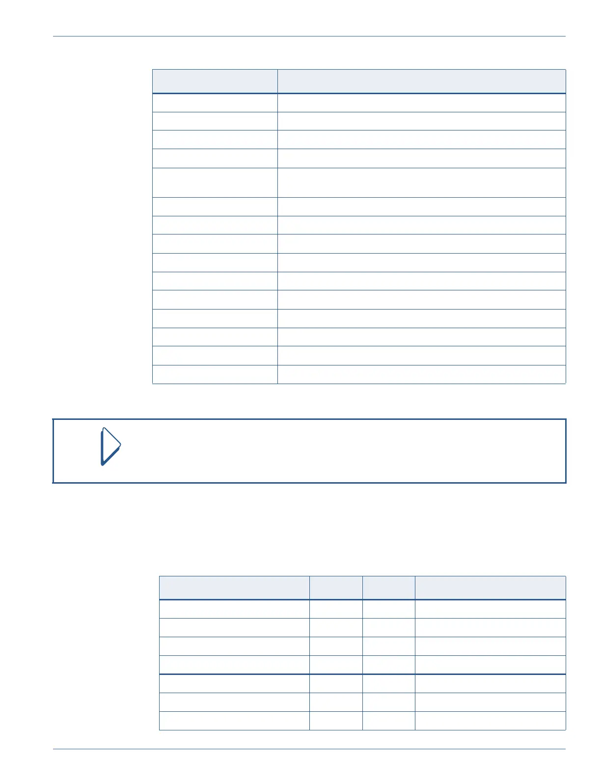
Table A.40: RTM Header Functions (Continued)
Header Number Description
Headers indicated as “Factory use only” are not intended for use in the field. Field operations
are not supported. All Headers and their functions are listed for completeness.
Table A.41: RTM PMC I/O (JB2) Pin Assignments
PMC J14 Pin (Odd Numbers) JB2 Pin JB2 Pin PMC J14 Pin (Even Numbers)
PMC_01 1 2 PMC_02
PMC_03 3 4 PMC_04
PMC_05 5 6 PMC_06
PMC_07 7 8 PMC_08
PMC_09 9 10 PMC_10
PMC_11 11 12 PMC_12
PMC_13 13 14 PMC_14
Artisan Technology Group - Quality Instrumentation ... Guaranteed | (888) 88-SOURCE | www.artisantg.com