HOST INTERFACE
Data Device Corporation DS-BU-67301B-G
www.ddc-web.com
1/14
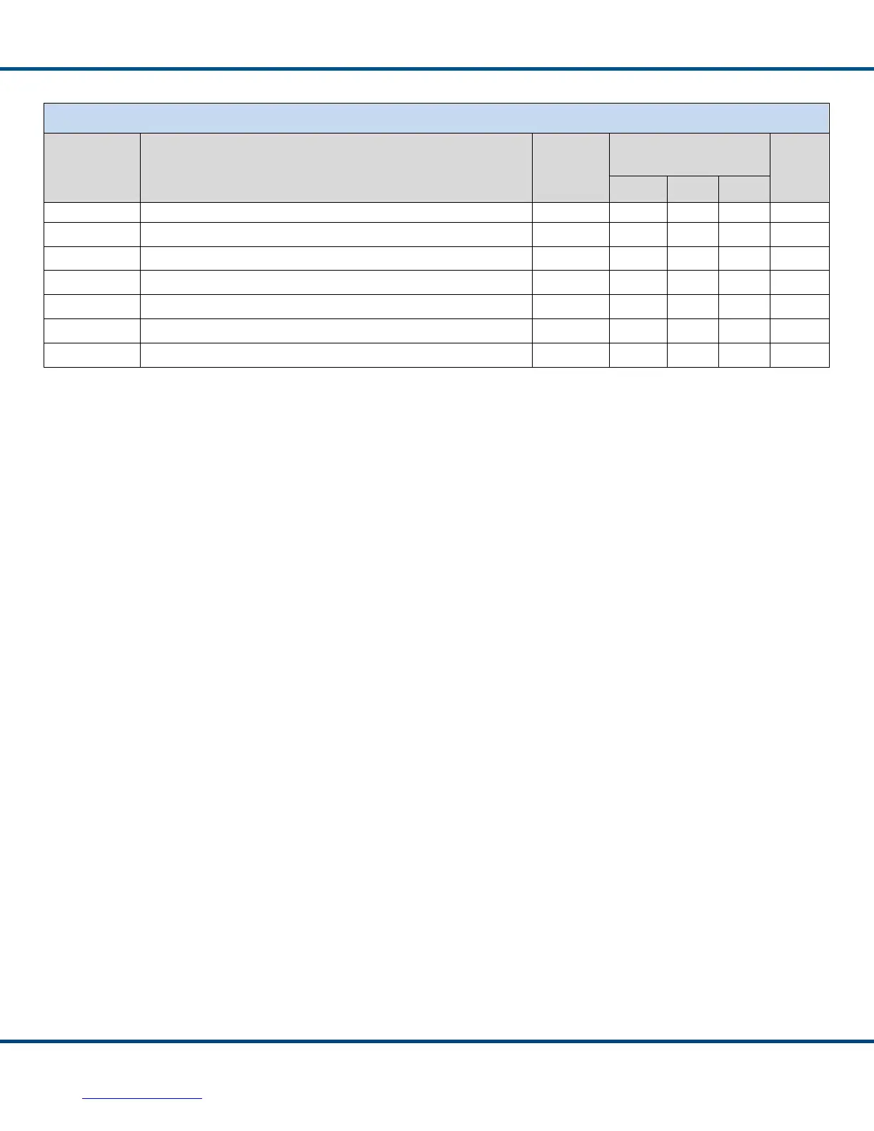
Table 7. Asynchronous Timing Information
REF DESCRIPTION NOTES
Timing
Characteristics
UNITS
MIN TYP MAX
t
RDD
nDATA_STRB high delay to nDATA_RDY high 10pF load 2 17 ns
t
OH
CPU_DATA output valid hold time following nDATA_STRB high 10pF load 2 ns
t
OHZ
nDATA_STRB high delay to CPU_DATA high-z 10pF load 17 ns
t
DS
CPU_DATA valid setup time prior to nDATA_STRB low 10 ns
t
DH
CPU_DATA valid hold time following nDATA_STRB high 0 ns
t
ALP
ADDR_LAT pulse width 40 ns
For the 32-bit Asynchronous timing diagrams, POL_SEL is assumed to be connected
to logic ‘0’. That is, RD_nWR = ‘1’ to read and ‘0’ to write.
For the 16-bit Asynchronous timing diagrams, POL_SEL is assumed to be connected
to logic ‘0’ and TRIG_SEL is assumed to be connected to logic ‘1’. For these
diagrams, the data indicated as “Data A” is bits 31:16, and is always transferred prior
to the data indicated as “Data B”, which is bits 15:0. For the 16-bit Asynchronous
timing diagrams, RD_nWR = ‘1’ to read and ‘0’ to write.
 Loading...